


Inside the Spartan-6: Using LUTs to optimize circuits
While building a small CPU on a Spartan-6 chip I came across the same old problem: my Verilog was mapping to a lot of slices . Way more then seems reasonable. So let's dig in and see what's really going on.
The J1 CPU (see Messing Around with a J1) is an amazingly streamlined design expressed in just over 100 lines of Verilog, and is reasonably compact at 150 Spartan-6 slices (half of that with the modifications described in the article). But the Picoblaze is packed into 26 slices. How did they do it? Simple muxes I've coded in HDLs are often this size. It appears that the Xilinx ISE synthesis tool is not that good at optimizing logic at least in some cases. Some magic is required.
I isolated a piece of verilog, a small logic ALU, into a separate module:
module alu_log
  (input en,
   input [2:0]   op,
   input [17:0]  tos,
   input [17:0]  nos,
   output reg[17:0] res);
   always @(en or op or nos or tos)
     if(sel)
       case (op)
         3'b000: res = nos & tos;          // and
         3'b001: res = nos | tos;         // or
         3'b010: res = nos ^ tos;        // xor
         3'b011: res = ~tos;            // invert
         3'b100: res = tos;            // dup
         3'b101: res = nos;           // drop
         3'b110: res = nos;          // over
         3'b111: res = nos;         // swap
         default: res = tos;
       endcase
     else
       res = 18'h000;
endmodule // alu_log
This is a logic ALU, controlled by a 3-bit opcode. Since my CPU is a stack machine, the operands are always limited to TOS and NOS. I also reserve a way to silence the ALU with a single-bit enable.
What is this circuit? Superficially, it looks like a 16-1 mux, or an 8-1 mux with an enable. However, there are only 2 inputs, so it should be represented more compactly. Personally I think it should be a lookup table mapping directly to a 6-input LUT on the Spartan-6. 18 LUTS, one per bit, should fit into 4 ½ Spartan-6 slices.
Does each bit fit into a LUT? It should. Taking an inventory, we have: 1 (EN), 3 (OP), 1 (TOS) and 1 (NOS) bits per LUT – exactly 6. Let us see what Xilinx thinks.
In order to avoid merging this module with the rest of the circuit, Xilinx tools need to be notified to keep the modules separate. If you dig into the extensive Xilinx documentation, you will find that XST, the synthesis tool, can be set to do so. In my case I have a whole file of parameters that XST loads, and inside it I placed:
-keep_hierarchy Yes
Looking at the .srp (the synthesis log) file:
Synthesizing
Unit <alu_log>.
Found 18-bit 7-to-1 multiplexer for signal <op[2]_nos[17]_wide_mux_4_OUT>
created at line 308.
   Summary:
   inferred
 2 Multiplexer(s).
7:1 multiplexer does not sound promising. Neither does the 'inferred 2 Multiplexers' notice in the summary. Looking in top.mrp (the mapping log) I see this:
+---------------------------------------------------------------------------------
| Module            | Partition | Slices*       | Slice Reg     | LUTs         |
+---------------------------------------------------------------------------------
| +alu_log          |           | 17/17         | 0/0           | 18/18        |
Hmm. That is not good.
Winning Through Instantiation
It looks like we have to somehow force Xilinx tools to make LUTs. The way to do it is through instantiation: instead of writing high-level verilog code and hoping that the tools infer what we want, we just write our code exactly as we want it to come out. Kind of like assembly language programming for FPGAs. There is a way to do that, right in your favorite HDL.
Look at the Xilinx manual known as UG615, Spartan-6 Libraries Guide for HDL Designs. It lists all the goodies inside the Spartan-6 FPGA with examples of how to instantiate them in Verilog and VHDL.
Doing this limits your design to the particular flavor of the Xilinx chip. That may be a problem, or a blessing, depending on your application. In my case it makes perfect sense, as I am looking to build a Xilinx-specific CPU.
Instantiation requires a fairly deep understanding of the FPGA architecture. It is not that hard to come by: study DS160, Spartan-6 Family Overview if you haven't. It is a delightful read, and full of illustrations.
Making a LUT-based circuit
So in the HDL Libraries Guide you will find this:
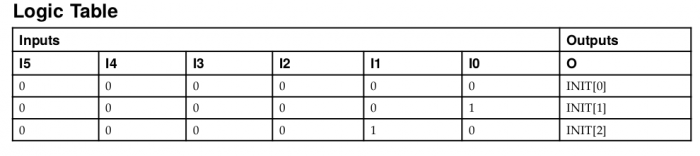
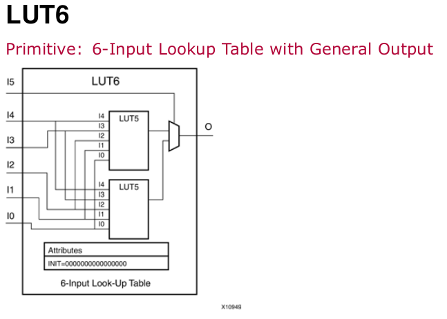 Note the logic table:
It continues all the way to INIT63 – there are 64 bits in the lookup table to initialize.
To instantiate a LUT6, this code must be placed into your Verilog file:
LUT6 #(
.INIT(64’h0000000000000000) // Specify LUT Contents
)
LUT6_inst (
.O(O),   // LUT general output
.I0(I0), // LUT input
.I1(I1), // LUT input
.I2(I2), // LUT input
.I3(I3), // LUT input
.I4(I4), // LUT input
.I5(I5)  // LUT input
);
The trick with a lookup table, of course, is to initialize it so that it outputs what you want. The lookup table is basically a 64-bit ROM with 6 address lines I0 through I5, and the result pops out the O wire. If the INIT is all 0's, O will always be 0. If the init is 64'h0000000000000001, O is always 0 except when I0==1, etc.
This is pretty cumbersome, so I usually use a paper worksheet made for this purpose, or a spreadsheet like this one(download spreadsheet):
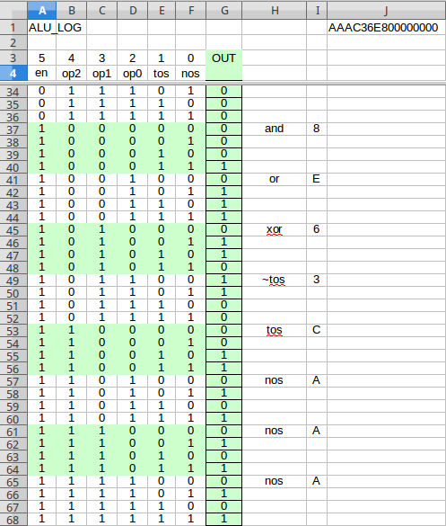
EN is I5, the top bit. When 0, the output is 0, so the first 32 lines are not shown (and the low 32 bits of INIT are 32'h00000000).
The remaining lines are just a lookup table of what happens when the I bits are set to various values. For each possible combination, write the desired result (0 or 1) into the OUT column. Then, starting at the bottom, write down the digits of the INIT; four bits at a time makes a hex digit. Or have the spreadsheet do it for you. In this case, the INIT is 64'hAAAC36E800000000.
Now it's a simple matter to instantiate the 18 LUTs, one per bit, in our module. The INIT is the same for every bit in this case. The arguments to LUT6 are passed backwards, just to make your life even more interesting (OUT,I5,I4,I3,I2,I1,I0).
module alu_log1
  (input en,
   input [2:0]   op,
   input [17:0]  tos,
   input [17:0]  nos,
   output [17:0] res);
  LUT6 #(.INIT(64'hAAAC36E8_00000000)) bit17(res[17], nos[17], tos[17], op[0],op[1],op[2],en);
  LUT6 #(.INIT(64'hAAAC36E8_00000000)) bit16(res[16], nos[16], tos[16], op[0],op[1],op[2],en);
  LUT6 #(.INIT(64'hAAAC36E8_00000000)) bit15(res[15], nos[15], tos[15], op[0],op[1],op[2],en);
  LUT6 #(.INIT(64'hAAAC36E8_00000000)) bit14(res[14], nos[14], tos[14], op[0],op[1],op[2],en);
  LUT6 #(.INIT(64'hAAAC36E8_00000000)) bit13(res[13], nos[13], tos[13], op[0],op[1],op[2],en);
  LUT6 #(.INIT(64'hAAAC36E8_00000000)) bit12(res[12], nos[12], tos[12], op[0],op[1],op[2],en);
  LUT6 #(.INIT(64'hAAAC36E8_00000000)) bit11(res[11], nos[11], tos[11], op[0],op[1],op[2],en);
  LUT6 #(.INIT(64'hAAAC36E8_00000000)) bit10(res[10], nos[10], tos[10], op[0],op[1],op[2],en);
  LUT6 #(.INIT(64'hAAAC36E8_00000000)) bit9 (res[ 9], nos[ 9], tos[ 9], op[0],op[1],op[2],en);
  LUT6 #(.INIT(64'hAAAC36E8_00000000)) bit8 (res[ 8], nos[ 8], tos[ 8], op[0],op[1],op[2],en);
  LUT6 #(.INIT(64'hAAAC36E8_00000000)) bit7 (res[ 7], nos[ 7], tos[ 7], op[0],op[1],op[2],en);
  LUT6 #(.INIT(64'hAAAC36E8_00000000)) bit6 (res[ 6], nos[ 6], tos[ 6], op[0],op[1],op[2],en);
  LUT6 #(.INIT(64'hAAAC36E8_00000000)) bit5 (res[ 5], nos[ 5], tos[ 5], op[0],op[1],op[2],en);
  LUT6 #(.INIT(64'hAAAC36E8_00000000)) bit4 (res[ 4], nos[ 4], tos[ 4], op[0],op[1],op[2],en);
  LUT6 #(.INIT(64'hAAAC36E8_00000000)) bit3 (res[ 3], nos[ 3], tos[ 3], op[0],op[1],op[2],en);
  LUT6 #(.INIT(64'hAAAC36E8_00000000)) bit2 (res[ 2], nos[ 2], tos[ 2], op[0],op[1],op[2],en);
  LUT6 #(.INIT(64'hAAAC36E8_00000000)) bit1 (res[ 1], nos[ 1], tos[ 1], op[0],op[1],op[2],en);
  LUT6 #(.INIT(64'hAAAC36E8_00000000)) bit0 (res[ 0], nos[ 0], tos[ 0], op[0],op[1],op[2],en);
endmodule
This looks dense and intimidating, doesn't it? It pays to save this instantiation step until the last possible moment, as making changes here is a little painful. Keep your original verilog module next to this new one, so you can figure out what it does. Comments are pretty much required, as there is nothing in this module to indicate its actual function.
Let's see what it maps to. The .mrp file reports...
+---------------------------------------------------------------------------------
| Module            | Partition | Slices*       | Slice Reg     | LUTs         |
+---------------------------------------------------------------------------------
| +alu_log          |           | 16/16         | 0/0           | 18/18        |
Wait, a minute, still 16 slices. WTF?
The .srp file no longer shows the 7:1 mux, so let's open the FPGA editor and find the slices. OK, it appears that although we are packing a LUT per bit correctly, most LUTs are littered all over the place, each taking up a whole slice. Perhaps it makes the router's job easier to spread out the LUTs in such environmentally hoggish way.
I still want to pack it into 4 1/2 slices. What now?
Manual Placing
Luckily, Xilinx tools allow us to use placement constraints. Digging through the manual you will find the RLOC constraint that allows us to locate parts within a module. RLOC is a relative location constraint, and we specify the location in X and Y coordinate space relative to some arbitrary position, good enough for now, since we just want to glue the LUT stack together.
The manuals provide some information about the various grid coordinates for slices and LUTs within. The easiest way to figure it out for sure is with the FPGA editor. The important thing to remember is that each slice contains 4 LUTs, so each group of four LUTs will have the same coordinates.
The new code for the module:
module alu_log2
  (input sel,
   input [2:0]      op,
   input [17:0]  tos,
   input [17:0]  nos,
   output [17:0] res);
  (*RLOC="X0Y4"*) LUT6 #(.INIT(64'hAAAC36E8_00000000)) bit17(res[17], nos[17], tos[17], op[0],op[1],op[2],en);
  (*RLOC="X0Y4"*) LUT6 #(.INIT(64'hAAAC36E8_00000000)) bit16(res[16], nos[16], tos[16], op[0],op[1],op[2],en);
  (*RLOC="X0Y3"*) LUT6 #(.INIT(64'hAAAC36E8_00000000)) bit15(res[15], nos[15], tos[15], op[0],op[1],op[2],en);
  (*RLOC="X0Y3"*) LUT6 #(.INIT(64'hAAAC36E8_00000000)) bit14(res[14], nos[14], tos[14], op[0],op[1],op[2],en);
  (*RLOC="X0Y3"*) LUT6 #(.INIT(64'hAAAC36E8_00000000)) bit13(res[13], nos[13], tos[13], op[0],op[1],op[2],en);
  (*RLOC="X0Y3"*) LUT6 #(.INIT(64'hAAAC36E8_00000000)) bit12(res[12], nos[12], tos[12], op[0],op[1],op[2],en);
  (*RLOC="X0Y2"*) LUT6 #(.INIT(64'hAAAC36E8_00000000)) bit11(res[11], nos[11], tos[11], op[0],op[1],op[2],en);
  (*RLOC="X0Y2"*) LUT6 #(.INIT(64'hAAAC36E8_00000000)) bit10(res[10], nos[10], tos[10], op[0],op[1],op[2],en);
  (*RLOC="X0Y2"*) LUT6 #(.INIT(64'hAAAC36E8_00000000)) bit9 (res[ 9], nos[ 9], tos[ 9], op[0],op[1],op[2],en);
  (*RLOC="X0Y2"*) LUT6 #(.INIT(64'hAAAC36E8_00000000)) bit8 (res[ 8], nos[ 8], tos[ 8], op[0],op[1],op[2],en);
  (*RLOC="X0Y1"*) LUT6 #(.INIT(64'hAAAC36E8_00000000)) bit7 (res[ 7], nos[ 7], tos[ 7], op[0],op[1],op[2],en);
  (*RLOC="X0Y1"*) LUT6 #(.INIT(64'hAAAC36E8_00000000)) bit6 (res[ 6], nos[ 6], tos[ 6], op[0],op[1],op[2],en);
  (*RLOC="X0Y1"*) LUT6 #(.INIT(64'hAAAC36E8_00000000)) bit5 (res[ 5], nos[ 5], tos[ 5], op[0],op[1],op[2],en);
  (*RLOC="X0Y1"*) LUT6 #(.INIT(64'hAAAC36E8_00000000)) bit4 (res[ 4], nos[ 4], tos[ 4], op[0],op[1],op[2],en);
  (*RLOC="X0Y0"*) LUT6 #(.INIT(64'HAAAC36E8_00000000)) bit3 (res[ 3], nos[ 3], tos[ 3], OP[0],OP[1],OP[2],en);
  (*RLOC="X0Y0"*) LUT6 #(.INIT(64'HAAAC36E8_00000000)) bit2 (res[ 2], nos[ 2], tos[ 2], OP[0],OP[1],OP[2],en);
  (*RLOC="X0Y0"*) LUT6 #(.INIT(64'HAAAC36E8_00000000)) bit1 (res[ 1], nos[ 1], tos[ 1], OP[0],OP[1],OP[2],en);
  (*RLOC="X0Y0"*) LUT6 #(.INIT(64'HAAAC36E8_00000000)) bit0 (res[ 0], nos[ 0], tos[ 0], OP[0],OP[1],OP[2],en);
ENDMODULE
Note that the module is arranged down from bit 17 to bit 0. The LUT RLOC stack should be ordered in the same direction, bit 0 at the bottom. Although it does not matter much in this case, the arithmetic ALU will use carry chains that bubble up from the bottom.
Let's look at the map report again.
+---------------------------------------------------------------------------------
| Module            | Partition | Slices*       | Slice Reg     | LUTs
+---------------------------------------------------------------------------------
| +alu_log          |           | 5/5           | 0/0           | 18/18
5 slices. Much better than 16.
It's possible to use the verilog generate statement to make a macro that automatically expands to as many bits as you need. Using it is a little problematic with the RLOC directive. Not worth it for our purposes, anyway.
It is also possible to create a generic ROM with Verilog. If you try it you will see why you don't want to do that - extracting bits vertically from the ROM array is perhaps even more painful than instantiating LUTs.
More Toys to Play With
Just look at this FPGA editor view of a Spartan-6 MSLICE:
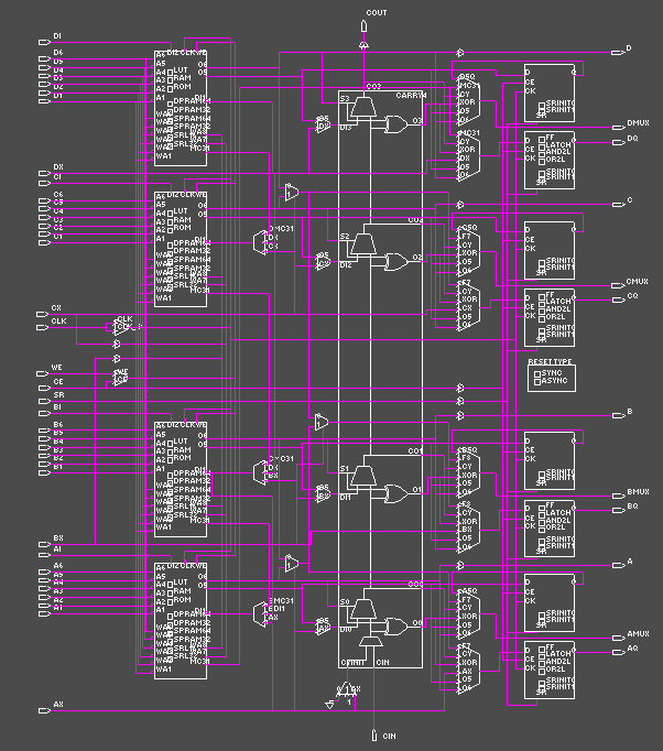
So far we are only using the LUTs, the rectangles on the left side. With instantiation, we can also use the carry chain, various muxes and all those flip-flops too.
Summary
Instantiation is an extremely powerful technique, resulting in compact circuits bound to the underlying hardware. Much like using assembly language, instantiating should be saved for specific modules requiring optimization, at the time optimization is necessary.
Many of my designs had benefited greatly from my ability to create strange muxes, (mis)using the carry chains and combining shift registers with other circuits inside the same slice.
Instantiation opens the door to the fullest utilization of the underlying FPGA fabric, and I look forward to writing more about instantiating Xilinx FPGA circuits. I hope you will give instantiation a try.


- Comments
- Write a Comment Select to add a comment
To post reply to a comment, click on the 'reply' button attached to each comment. To post a new comment (not a reply to a comment) check out the 'Write a Comment' tab at the top of the comments.
Please login (on the right) if you already have an account on this platform.
Otherwise, please use this form to register (free) an join one of the largest online community for Electrical/Embedded/DSP/FPGA/ML engineers:


