


Use Microprogramming to Save Resources and Increase Functionality
Introduction
Microprogramming is a design approach that every FPGA designer should have in their bag of tricks. I subscribe to the concept that microprogramming is a structured approach to the design of state machines. This is essentially the view of Maurice Wilkes when he first proposed microprogramming in 1951 as an alternative method for the implementation of the control section of a computer. Wilkes was interested in improving the reliability and reducing time needed to implement the control section of computers. In his time, the control sections of computers were hard-wired designs using random logic using ad hoc techniques. In other words, they were difficult to design, implement, and more importantly, test.
Wilkes faced the problem that the technology needed to efficiently implement his structured design approach was not available when he proposed it. It would not become available for 10 to 15 years after his original proposal. In the 1960s, a number of well known computer manufacturers such as IBM, Interdata, and others adopted his microprogramming concepts in their designs. The success of those efforts drove many other computer manufacturers to adopt the approach for their designs. Virtually all computers of the 1970s and 1980s used one form or another of microprogrammed controllers. Many microprocessors, including the Intel 8086 and Motorola 68000, used variations of Wilkes' concepts. Today, even with the large number of pipelined, hard-wired processors available, the industry leading processors from Intel continue to employ microprogramming in some form.
A great deal of material is available on the internet on this subject. Invariably it is aimed primarily at the implementation of computers or processors of one sort or another. This is an unfortunate result of the technique's success in implementing computers and microprocessors. Consequently, microprogramming is almost forgotten as a design approach that can be used for virtually any design requiring a state machine.
In the remainder of this article, I will describe a successful application of microprogramming to the implementation of a FIFO. Most designers would implement a FIFO, particularly a synchronous distributed RAM FIFO in SRAM-based Xilinx FPGAs, using simple counters and comparators. I too am in that camp, but this article will describe a situation and a solution in which I needed to employ an alternative to my normal problem solving approach, i.e. microprogramming.
The Problem
A number of years ago I found myself in a quandary. I had a virtually complete FPGA design in hand where its two 16550-compatible UARTs needed significantly deeper FIFOs. This new requirement came to light just before the project was about to be delivered: the absolutely worst time for a customer to change/add requirements. But without the additional depth, the customer's software would be unable to respond to interrupts at the rate needed to prevent FIFO overflow, and the receive data would be lost.
Therefore, following my normal practice, I simply modified my standard FIFOs designs to add the additional depth. Upon attempting to synthesize the design, I found that the modified design exceeded the available logic resources of the target part. Changing the FPGA was not an option, so I compromised and only increased the depth of the receive FIFOs.
Although the design with the asymmetric FIFOs fit, the resulting design used 100% of the logic resources of the FPGA. It probably would have been okay to go into production with that design, but the risk was too great to let that happen. Fortunately, the target FPGA had available a number of Block RAMs that could be used to recover some of the logic resources of the FPGA.
The Standard Approach
The data transfer rates and the timing between the requests on each interface convinced me that a time multiplexed FIFO was appropriate. FIFOs are one of those tools that are generally well understood and which have a generally accepted structure. In hardware, FIFOs are generally expected to accept inputs and provide outputs with no delay even when the controls are asserted simultaneously. However, in most real world situations, there can be a large disparity between the input and output rates.
This is particularly the case with the FIFOs in UARTs. On the processor side, the data is written and/or read using short access cycles on the order of four clock cycles. The period at which theses operations occur is generally equal to the period of four to six instructions, i.e. 16 to 24 clock cycles. On the UART side, the data is read and/or written at rates substantially slower. For example, with a reference clock 256 times faster than the baud rate, an asynchronous serial data stream using a 10 bit frame (1 start bit, 8 data bits, and 1 stop bit) will have a period of 2560 clock cycles between operations to the FIFO(s). These large access periods on both sides of the FIFO provide the opportunity to time multiplex the FIFO storage element and any computational elements like counters.
I was looking for any way to reduce the resource utilization of the FPGA, and one way to accomplish that objective is to time multiplex the control logic and partition the block RAM into two halves: one for transmit and the other for receive. The user side of the FIFOs connected to the I/O bus of a 29.4912 MHz AMD AM186ER microcomputer. For reads and writes of the FIFOs from the processor side I estimated that the best cycle time would be approximately 1 microsecond, and the processor-side FIFO read/write operations are mutually exclusive. The maximum bit rate the would be supported would be 115200 bps (256 clock cycles per bit), or 2560 clock cycles per character.
For several years I had been using the synchronous write capabilities of the Look-Up Table (LUT) RAMs in Xilinx FPGAs to implement storage elements instead of using discrete registers. Implementing 16 8-bit registers/storage locations only requires 8 LUTs and not 128 FFs as required when discrete registers are used. Furthermore, the built-in multiplexer associated with the LUT RAMs also saves a large amount of additional logic. Therefore, I decided to implement the FIFO's word count register, WCnt, write pointer, WPtr, and read pointer (RPtr) using distributed RAMs, i.e. LUT RAM. Since time multiplexed logic appeared to be an option, I decided to implement the customer's desired receive and transmit FIFO depth with one block RAM per UART, i.e. the receive and transmit FIFOs are also time multiplexed.
I had been avoiding using microprogramming since I did not have any tools available that I could use to "program" the microprogram. Without microprogramming on the menu, so to speak, I resorted to using the ABEL HDL to create a time-division multiplexed FIFO with 256 byte receive and 256 byte transmit depths. (The design was a Foundation 2.1i design implemented using schematics. Coregen was used extensively, and so were a number of company-developed library components such as the UARTs.)
The following table provides the results of this effort compared to the that of the LUT-based FIFO design:
| Place & Route Parameter | DPRAM-based FIFOs | BlkRAM-based FIFOs |
| Slices | 1728/1728 | 1728/1728 |
| Flip Flops | 1140 | 1158 |
| Latches | 32 | 32 |
| 4 Input LUTs | 1992 | 2324 |
| DPRAMs | 448 | 48 |
| 16x1 RAMs | - | 16 |
| Slices Used for Unrelated Logic | 193/1728 | 7/1728 |
| IOBs | 120/176 | 120/176 |
| IOB Flip Flops | 29 | 29 |
| IOB Latches | 8 | 8 |
| TBufs | 175/1828 | 175/1828 |
| Block RAMs | 0/12 | 2/12 |
| GCLKs | 4/4 | 4/4 |
| GCLK IOBs | 3/4 | 3/4 |
| RPM Macros | 14 | 16 |
| Gate Count | 80,150 | 65,560 |
| JTAG Gate Count | 5,904 | 5,904 |
The key parameters to consider are highlighted in the table. Specifically note the 100% utilization factor: 1728/1728 slices used. The FIFO registers are stored in 8 LUTs for each UART, and as expected 8 LUTs are shown as being configured as 16x1 RAMs. A significant decreased occurred in the DPRAM category with each UART losing the equivalent of 200 DPRAMs, which in the Xilinx FPGA family being used is equivalent to 400 16x1 LUTs for each UART of the original design. However, in terms of LUTs, the new Block RAM FIFO (with ABEL-based SM) exhibits a net gain of 400 LUTs.
Even though the part is fully utilized at the slice level, there is a decrease in the number of LUTs used in the design:
2*400-(2324-1992) = 468.
This is good news and further enhanced performance because the new design has also reduced the number of slices used for unrelated logic by 186 slices. All things considered, the new Block RAM FIFOs free up a good number of resources. However, the design requires distribution across all slices in the part. This means that it may be possible to stuff a bit more logic into the part, but it will not be easy and it won't be a significant function. Examining the PAR results in the Xilinx FPGA editor clearly demonstrated that the ABEL SM was the largest component of the FIFO with the largest area. The other elements of the new FIFO are optimized for the Xilinx architecture.
(Note: to the best of my recollection, Data I/O originally developed the language. ABEL competed with a number of other HDLs such as CUPL, PALasm, and AHDL. Xilinx purchased ABEL in order to compete with Altera's AHDL offering. I had used ABEL since the mid-80s, and it was a great tool for use with the PALs and CPLDs of the '80s and '90s. However, by the '00s, it was showing its age. All the major FPGA and CAD tool vendors had moved toward Verilog and VHDL, so as this FIFO design demonstrates, the optimization of ABEL for the Xilinx FPGA architecture was falling way behind other tools.)
The Microprogrammed Approach
One way to solve this problem is to use a microprogrammed SM to replace the FIFO control SM implemented using the ABEL HDL. Without a microassembler to provide an automatic way to generate the state table or ROM, it is necessary to encode the control fields in a manner that will make manual generation of the state table easy. With a working design using ABEL in place, I decided to use the same control fields for the microprogrammed SM.
With the control fields determined, the next decision necessary is how the state machine will determine the next state. There are many ways to do this. Various references, in book form or on-line, provide good discussions of the various techniques. In the case of this design, the objective is simplicity, so instead of using as microprogram sequencer or loadable counter, I opted to simply encode the next state as a field in the microprogram control word. Some means must be provided for making decisions regarding the next state. The approach that I decided to use for this project is to use a priority encoder whose outputs directly encode the next state of the SM. To enable the priority encoder, I use the IDLE state of the SM.
I used a priority encoder in order to provide a way to ensure that the host side data is written into the FIFO before it can be overwritten. In addition, I wanted to provide read data to the host processor from the FIFO without requiring wait states. In this case, a no wait state memory cycle is 4 cycles of the host processor's clock.
The ABEL state machine could read and write the FIFO in an average of two or three processor memory cycles. So the microprogrammed SM must provide the same performance. If the interfaces of the microprogrammed SM matched those of the ABEL SM, then the microprogrammed SM could simply be dropped into the existing ABEL-based FIFO design. I chose this option because it would be more efficient than a new approach, and I didn't have much time to solve the FIFO depth problem of the FPGA UARTs.
Figure 1: A block diagram of the Block RAM FIFO
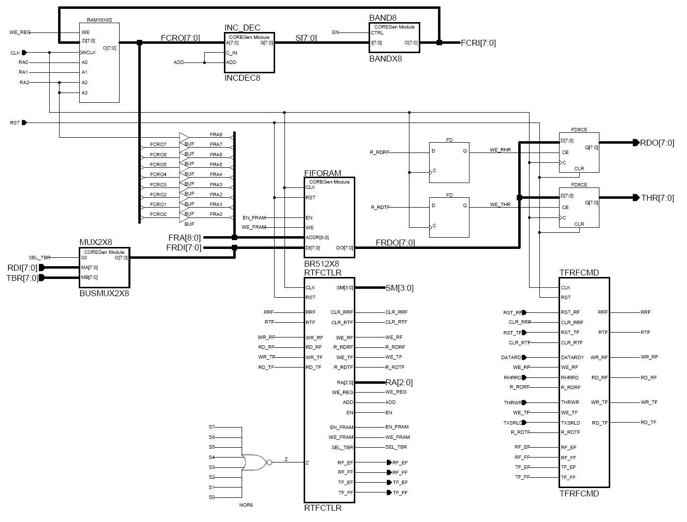
A block diagram of the block RAM FIFO, with the microprogrammed SM in place of the ABEL SM, is shown in the Figure 1. As can be seen, the distributed RAM (LUTs) holding the word counter, write pointer, and read pointer for each FIFO is in the upper left of the diagram. An adder/subtractor followed by a bus AND provide the arithmetic functions needed to increment/decrement the word counter, increment the write and read pointers, and to clear these registers when a reset is issued. In the center is found the FIFO's Block RAM storage element, and to its left is a multiplexer for writing receive data from the UART, or transmit data from the host processor. To the right of the Block RAM are the FIFO's two output data registers. The write strobes for these output registers are delayed by one cycle to accommodate the Block RAM's one cycle read delay. In the lower center is the FIFO's control SM, and to its right are the request flag registers. The request flag registers hold read/write requests from the host interface or from the UART's Rx/Tx SMs.
Conceptually, this FIFO follows a standard model. Since it is replacing FIFOs built from LUTs, the output register must hold the output of the memory cell pointed to by the read pointer. Thus, when a write is made to an empty FIFO, the data is written into the storage element and the write pointer is advanced. Then that data is read and written to the appropriate output register and the read pointer is advanced. Finally, the word counter is incremented and the empty flag is adjusted.
Because a single ported RAM is used for holding the registers, the controller must read the register from the RAM, update the value as needed using the adder/subtractor and bus AND functions, and write it back into the RAM. The design performs these actions in a single clock cycle. This allows FIFO reads and writes to be performed in 2 clock cycles, except for writes to empty FIFOs which require a total of 3 cycles to perform.
Figure 2: A block diagram of the microprogrammed SM
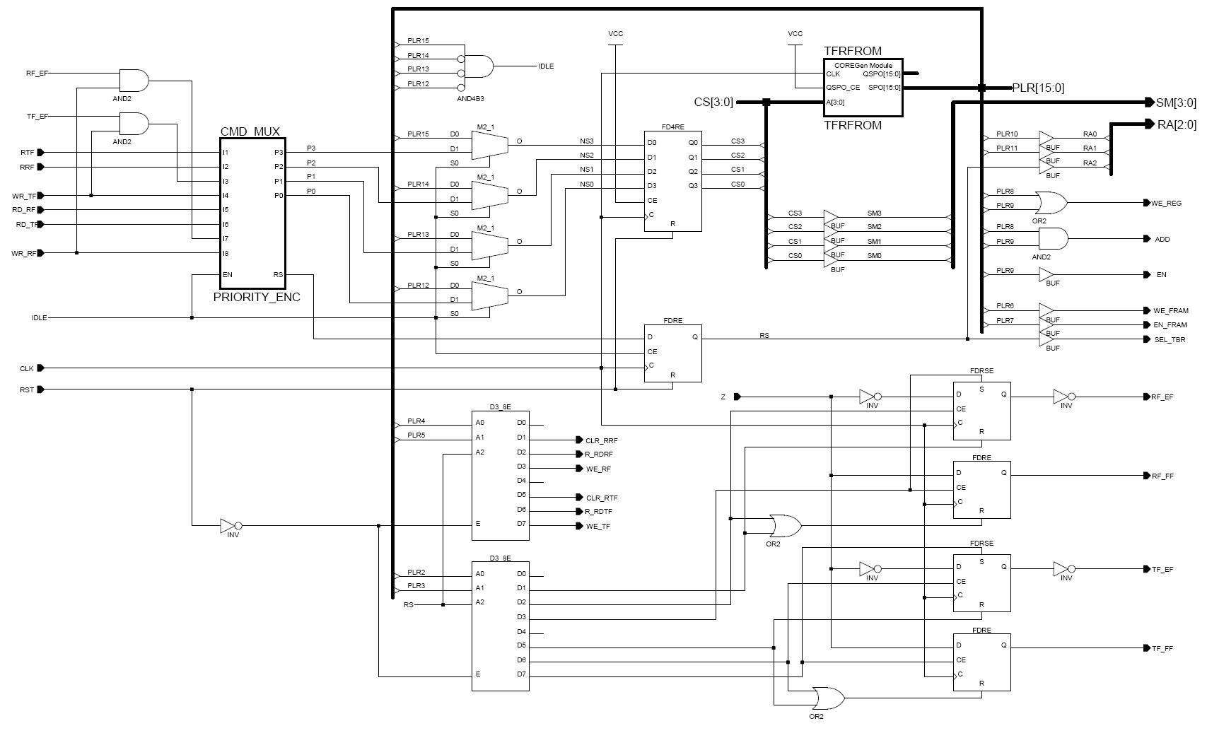
A block diagram of the microprogrammed SM is provided in Figure 2. External to the module, the read/write service requests are qualified for the reads from empty FIFOs or writes to full FIFOs are ignored. In the top left resides the priority encoder. The two AND gates generate the requests to write empty Rx/Tx FIFOs. In the top center, a 4-input AND gate decodes the NS (next state) field and generates the IDLE signal which enables the priority encoder and controls the four 2:1 multiplexers that supply the CS (current state) register. The CS register provides the address into the state table, i.e. the microprogram ROM. The loop formed by the NS field, the 2:1 multiplexers, and the CS register is all that is required to implement the rudimentary microprogrammed SM needed for this application. The various decoders, and individual gates placed on the state table's output bus provide the mapping of the encoded control fields to the control signals needed to control the FIFO. In the bottom right are the four FIFO flag registers. With careful implementation of the control sequences, only a single comparator (which is implemented using a single 8-input AND gate) is needed to set the empty and full flags. Since the FIFO's read/write operations are serialized, comparison of the read and write pointers is not required. Instead, only zero testing of the word counter is required to set the FIFO flags. For example, if during a FIFO write, the word counter is zero after incrementing, it has wrapped around and the FIFO is full.
The following table defines the 16-bit microprogram word. (Only 14 bits are used in the application, but at the time I created the ROM in CoreGen, I decided to create a wider memory to allow growth if it became necessary.)
| Encoding | REG | ROP | RAM | ACK | FLAG |
| 00 | WCnt | NOP | NOP | NOP | NOP |
| 01 | Rsvd | Clear | Rsvd | Clear | Clear |
| 10 | WPtr | Dec | Read | Read | SetEF |
| 11 | RPtr | Inc | Write | Write | SetFF |
The following list provides a description of the control fields in the microword:
- The REG field defines the address of the FIFO register in the LUT-based register file: word counter, write pointer, and read pointer;
- The ROP field controls the operation that the adder/subtractor and bus AND provide on the register value: clear, increment, and decrement;
- The RAM field controls the operation performed on the FIFO's block RAM storage element: read, and write;
- The ACK field provides the acknowledge to the service request latches (and external module); the ACK Clear output allows the SM to clear all pending requests during a FIFO reset operation;
- The FLAG field controls the FIFO flag registers; the FLAG Clear output allows the SM to clear the FIFO Full flag and set the FIFO Empty Flag when a FIFO reset operation is requested.
The full microword consists of 4 NS select bits prepended to the 10 control bits described in Table 2. (Each of the 16 elements of the microprogram ROM is null padded to 16 bits.) Thus, each location in the microprogram ROM is represented by the following bit vector:
{NS[3:0], REG[1:0], ROP[1;0], RAM[1:0], ACK[1:0], FLAG[1:0], Rsvd[1:0]}
Because the CS register is reset automatically on configuration, the first four locations of the ROM are reserved for the FIFO reset microroutine. The state table consists of five sequences:
- FIFO reset sequence (CS=0..3);
- not empty FIFO write sequence (CS=4..5);
- FIFO read sequence (CS=6..7);
- SM Idle state (CS=8);
- empty FIFO write sequence (CS=9..11);
The FIFO reset sequence initializes each of the FIFO registers, clears any pending service requests, and initializes the FIFO flag registers. The not empty FIFO write sequence writes the data into the FIFO storage element while incrementing the write pointer, increments the word count, and sets the FIFO full flag to correct state. The FIFO read sequence reads the FIFO storage element (a delay FF aligns the memory read strobe with the output data from the block RAM and writes the data into the output register), increments the read pointer, decrements the word count, and set the FIFO empty flag to the correct state. The SM idle state waits until the priority encoder provides a non-idle NS code. The empty FIFO write sequence writes to the storage element and increments the write pointer, reads the storage element and increments the read pointer (and writes the output register after a one cycle delay), increments the word counter, and sets the FIFO empty flag to the correct state.
These sequences are used to support both the receive and transmit FIFOs. The time division multiplexing incorporated into this design saves a lot of resources. The complete microprogram is provided below in Table 3:
| Description | CS | NS | REG | ROP | RAM | ACK | FLG |
| Clear WCnt | 0000 | 0001 | WCnt | Clr | NOP | NOP | NOP |
| Clear Rsvd Register | 0001 | 0010 | Rsvd | Clr | NOP | NOP | NOP |
| Clear WPtr | 0010 | 0011 | WPtr | Clr | NOP | Clear | Clear |
| Clear RPtr | 0011 | 1000 | RPtr | Clr | NOP | NOP | NOP |
| Increment WPtr, Write RAM, Ack Write Rqst | 0100 | 0101 | WPtr | Inc | Write | Write | NOP |
| Increment WCnt, Set Full Flag | 0101 | 1000 | WCnt | Inc | NOP | NOP | SetFF |
| Decrement WCnt, Ack Read Rqst, Set Empty Flag | 0110 | 0111 | WCnt | Dec | NOP | Read | SetEF |
| Increment RPtr, Read RAM | 0111 | 1000 | RPtr | Inc | Read | NOP | NOP |
| Idle | 1000 | 1000 | WCnt | NOP | NOP | NOP | NOP |
| Increment WPtr, Write RAM, Ack Wr Rqst | 1001 | 1010 | WPtr | Inc | Write | Write | NOP |
| Increment RPtr, Read RAM, Ack Rd Rqst | 1010 | 1011 | RPtr | Inc | Read | Read | NOP |
| Increment WCnt, Set Empty Flag | 1011 | 1000 | WCnt | Inc | NOP | NOP | SetFF |
| Goto Idle | 1100 | 1000 | WCnt | NOP | NOP | NOP | NOP |
| Goto Idle | 1101 | 1000 | WCnt | NOP | NOP | NOP | NOP |
| Goto Idle | 1110 | 1000 | WCnt | NOP | NOP | NOP | NOP |
| Goto Idle | 1111 | 1000 | WCnt | NOP | NOP | NOP | NOP |
Table 4 below compares the FIFO resource utilization of the three approaches:
| FIFO Module | DPRAM-based FIFOs | BlkRAM+ABEL FIFOs | BlkRAM+ROM FIFOs |
| DFFs | 52 | 61 | 47 |
| FGs | 189 | 403 | 100 |
| CYs | - | 8 | 8 |
| DPRAMs | 200 | - | - |
| MEM16s | - | 8 | 8 |
| BlkRAMs | - | 1 | 1 |
The important results are the reduction in the number of DPRAMs, which are each equivalent to 2 LUTs or FGs. The reduction achieved represents a significant increase in the available resources in the FPGA. I no longer have easy access to the complete resource utilization report for the full FPGA project, but this effort freed up approximately 25% of the FPGA. Further, it made the FIFOs much deeper than those of the original design, and allowed the customer more time to process interrupts from incoming data.
A Verilog Implementation of Both Approaches
For those that may be skeptical of these results because they were determined for a design implemented with schematics, I have reimplemented both of these block RAM FIFOs using Verilog. One is implemented with a standard state machine paradigm and the other using the microprogramming paradigm described above. The HDL source, microprogram sources, and self-checking testbenches can be found in this GitHUB repository. I've compared the results in Table 5 below:
| FIFO Module | BlkRAM+SM FIFOs | BlkRAM+ROM FIFOs |
| FFs | 76 | 20 |
| 4-input LUTs | 163 | 101 |
| Occupied Slices | 127 | 63 |
| 16x1 RAMs | - | 8 |
| BlkRAMs | 1 | 1 |
Even with a more modern implementation in Verilog, the microprogrammed approach still results in a smaller design. The state machine implementation was automatically optimized by the synthesizer into a one-hot implementation. In both state machines only a total of 12 states were explicitly used. The self-checking testbenches provided are identical except for the instantiation of the UUT. On the plus side for the standard state machine is the fact that the synthesizer reports it as being approximately 8.5% faster than the microprogrammed state machine in a Spartan 3A -5 FPGA. In the application described in this article, the potential advantage offered by microprogramming is not as pronounced (~2:1) as it can be because the problem being tackled is fairly small to start with. In more complicated designs, I've been able to achieve a compression ratio as high as 4:1.
Summary
I use microprogrammed state machines for applications which require complex state machines. Recently to better support microprogramming, I had a simple microassembler developed. If you decide the try out microprogramming as described in this article, you may want to consider giving the microassembler a try. You can find the Windows executable on GitHUB.
The microprogram assembler was used to develop the memory initialization file used in the Verilog microprogrammed SM. It is presently written in C# and available only as a Windows executable. We are in the process of converting it to a console application in C++ and hope to have it available for Windows and Linux in a few weeks. There are a number of library/built-in elements in C# used in the current assembler that will require some work to convert to C++.
Comments on the subject presented are appreciated. I hope this article is thought provoking, and encourages some of you to consider using a previously well known and accepted approach for logic design. I was not exposed to microprogramming as an undergraduate EE student, and there are plenty of good references on-line and in print that can provide additional information to get you started. Mark Smotherman's on-line article, "A Brief History of Microprogramming", is a good place to start and includes a comprehensive reference list. I have also included a list of some of the references that I use.
What's Next
For my next article, I am planning to describe how to use an FPGA's LUTs to implement 12-16 asynchronous receivers in about the same area as a standard 16550-compatible UART. Like the Rx/Tx FIFO, that implementation was also schematic-based as well as microprogrammed. I will convert it to Verilog for the article.
References
- Andrews, Michael, Principles of Firmware Engineering, Potomac, MD, Computer Science Press, 1980
- Fairchild Semiconductor, Macrologic Bipolar Microprocessor Data Book, Mountain View, CA, Fairchild Camera and Instrument Corporation, 1976
- Advanced Micro Devices, Bipolar Microprocessor Logic and Interface Data Book, Sunnyvale, CA, Advanced Micro Devices, Inc., 1985
- Lynch, Michel A, Microprogrammed State Machine Design, Boca Raton, FL, CRC Press, Inc., 1993
- Mick, John and James Brick, Bit-Slice Microprocessor Design, New York, NY, McGraw-Hill Book Company, 1980
- Sondak, Norman and Efrem Mallach, ed., Microprogramming, Artech House, Inc. 1977
- White, Donnamaie E., Bit-Slice Design: Controllers and ALUs, New York, NY, Garland STPM Press, 1981
- Habib Stanley, ed., Microprogramming and Firmware Engineering Methods, New York, NY, Van Nostrand Reinhold, 1988
- Kraft, George D. and Wing N. Toy, Microprogrammed Control and Reliable Design of Small Computers, Englewood Cliffs, NJ, Prentice-Hall, Inc., 1981
- Husson, Samir S., Microprogramming: Principles and Practices, Englewood Cliffs, NJ, Prentice-Hall, Inc. 1970
© 2015 Michael A. Morris, All Rights Reserved.


- Comments
- Write a Comment Select to add a comment
To post reply to a comment, click on the 'reply' button attached to each comment. To post a new comment (not a reply to a comment) check out the 'Write a Comment' tab at the top of the comments.
Please login (on the right) if you already have an account on this platform.
Otherwise, please use this form to register (free) an join one of the largest online community for Electrical/Embedded/DSP/FPGA/ML engineers:


