


BGA and QFP at Home 1 - A Practical Guide.
It is almost universally accepted by the hobbyists that you can't work with high-density packages at home. That is entirely incorrect. I've been assembling and reflowing BGA circuit boards at home for a few years now. BGAs and 0.5mm-pitch QFPs are well within the realm of a determined amateur.
This series of articles presents practical information on designing and assembling boards with high-density packages at home. While the focus is on FPGA packages, most of the information applies equally well to any BGA and QFP package.
Introduction - Can't Be Done?
Before trying to actually solder a BGA chip at home, I did a lot of research and talked to many professionals. I was told that it's impossible to do - the task requires expensive placement, stenciling and precision reflow equipment, not to mention X-ray machines for quality control. I was told that you need 6-layer PCBs. However, I've made dozens of perfectly working 2-layer BGA boards without anything they would consider required equipment. I haven't had a hidden failure in dozens of boards I have running around the house.
Working with FPGAs and microprocessors requires surprisingly little investment. These chips indeed look extremely intimidating, especially the BGAs. However, they can be soldered with little effort on an inexpensive hotplate or a in a toaster oven. Oddly enough, BGAs are in many ways easier and more forgiving than the little QFP packages. You can even bake a BGA breakout board without ever making a stencil, applying solder paste or touching a soldering iron!
I spent a lot of time searching the net for a common-sense guide to hacking BGA boards. What I found was little snippets and hints. I promised myself that if I ever got good at reflowing my own boards I would put together a simple guide for others (and myself!). Here it is. Hopefully you will be encouraged and inspired to make your own project incorporating an FPGA.
Amateur Hour
Before delving into the depths of the subject, I would like to reiterate that these techniques are practical for the amateur. The word 'amateur' has all kinds of negative connotations in our society, so I would like to reclaim it. The actual meaning of the word is 'lover of'; amateurs love what they do, and do it for enjoyment rather then profit. There is not much to complain about with that definition.
However, the word 'amateurish' evokes an extremely negative sentiment. The assumption is that a 'trained professional' will always do a better job. That is often true, but not always. I will point to my "professionalish" TV set that crashes twice a week, and my "professionalish" car that often needs to be rebooted. Don't even start me on the subject of modern PC hardware and software. There was very little love involved in designing these items.
The truth is that professionals do it for money. They may not even like what they do, but it provides for their family. They are concerned with job security, office politics, standards compliance and keeping high manufacturing yields. Their designs have to work in hospitals and airplanes. Their employers have to comply with OSHA regulations. They are generally funded enough to afford specialized equipment. The ideas of non-standard approaches, using unorthodox equipment and coming up with brilliant designs or low-cost techniques is not as important - it's hard enough just to make something work on a tight deadline.
The amateur operates in an entirely different space. Money matters; time is less important. Real equipment designed for the job is entirely out of our reach. But we can be extremely clever - no one is going to fire us if we are wrong. We can punk it with toaster ovens and paper stencils. If the design is wrong, we can throw it away and take a loss of a few tens of dollars. We have no deadlines. If one out of four boards does not work - whatever, a lesson learned. We can bottom-pick outdated chips that no professional would touch in a new design.
And don't forget, we love doing it.
WHY BOTHER?
Why would anyone bother making an FPGA-based board at home? Surely there are many devboards that are affordable!
Most importantly, because it's fun. There is an incredible sense of accomplishment from making your own board. You will amaze your friends showing off FPGA boards you bake in your toaster oven.
There are other reasons. Devboards are fine and often affordable for one-off projects. But what if you need a few copies of your project? Or a couple of dozen? That quickly becomes very expensive.
FPGA devboards are often meant to show off a particular generation of an FPGA. A year later you may not be able to find another board! It also seems that the latest generation of cheap devboards is leaning towards little accessible IO, dense connectors and USB instead of the generous 100-mil connectors of yesteryear.
Finally, devboards may not have the mix of hardware you need for your project. Making your own board guarantees that you will get exactly what you want.
TOPICS
In order to create a successful FPGA-based board at home, the following concepts must be addressed:
- Modular design
- PCB fabrication
- PCB design
- Tools of the trade
- Your workspace
- Stencils
- Solderpasting
- Placing the chips
- Reflow
- Testing
Each of these is a formidable topic deserving attention, and I will address all these topics in future articles. I will focus specifically on the aspects that matter to our home manufacturing facility.
As I mentioned before, the professionals have a different agenda and I hope they will be more amused then upset with my lack of orthodoxy.
MODULAR DESIGN
Assuming that large BGA and QFP packages are problematic, it makes sense to partition your projects in a way that minimizes potential failure points. That leads to the inevitable conclusion that, at least while you are perfecting your process, you should limit each board to a single BGA.
Making and debugging breakout boards is a lot less stressful than a densely packed large board. In particular, BGA breakout boards require the least effort.
Your breakout boards can be tested separately and connected together with an inexpensive homemade PC board or better yet, wire-wrapped. Yes, wire-wrapped! Wire wrapping is enjoyable, reliable and easily changed. You may find that you misunderstood some of the wiring requirements and change your design without ordering and reflowing new boards.
The incremental cost of making a new board is low, so once everything works, you can design a new board containing all the components necessary. If you design your breakout boards wisely, you'll be able to easily combine them without too much layout work. By then you'll be pretty good at reflowing complicated packages, improving your chances of a successful final board.
The prototype breakout boards will then be available for new projects. You will probably have all kinds of ideas by the time your original project is done. It's a win-win situation.
A quick note on solderless breadboards. Attractive as they may seem, try to avoid them, except for very simple experiments. These things are atrocious, noisy and unreliable. My attempts to use them rarely ended well.
PCB FABRICATION
In my experience, it is not worth etching your own boards with FPGAs on them. I've etched hundreds of boards on previous occasions, but it is just not worth it with high-density chips. I've heard of people making 8-mil traces consistently - good enough for both 0.5mm QFP and 1mm BGA, but these traces have to be perfect. Soldermask helps a lot as well, an an even layer of tin-plating is a must. Even if the board is etched perfectly, home-etched PCBs are harder to solder, and we need all the help we can get. This is one area where professionally-made boards are in fact better.
The place for homemade boards is in providing 'motherboards' for your breakout boards. Very often, that will be enough for your project. This technique is extremely useful, and if you are smart you'll be able to avoid many long delays associated with low-cost PCB manufacturers.
Until recently it was fairly expensive ($100 and up) to have even small PCBs made by a prototype shop because of steep setup charges. Now there are cheaper alternatives. My favorite is oshpark.com - they make beautiful boards for a very reasonable price - around $1.67 per square inch with free shipping! It takes about 2-3 weeks to get the boards. There are even cheaper alternatives in China, but expect to wait a month for your design, and the quality may not be as good.
The PCB manufacturer's advertised trace sizes should be taken with a grain of salt. It's always wise to use the widest traces possible.
BGAs really don't appreciate any flexibility in your boards. Keep the boards thick - 1.6mm is pretty good for small boards.
PCB DESIGN
Chip Selection
I am assuming that you have a pretty good idea of what size FPGA you need for your project. If you don't, it's probably wise to prototype your circuit on a factory-made devboard to get a sense of how big the FPGA needs to be.
There are serious limits to what is possible with an inexpensive board. For instance, it is not possible to route all the pins of a large BGA on a 2-layer board. Large PC boards are expensive to manufacture, and larger FPGAs (requiring correspondingly larger breakout grids) will raise your costs.
An obvious observation is that smaller is easier. Fewer pins to solder means a smaller probability of wiring error or soldering failure. Not to mention a shorter design cycle and a much easier time testing later.
With FPGAs we have a fairly unusual opportunity - we have a choice of connecting only some of the most accessible pins. Connecting only some of the databus pins of a microprocessor won't do. So it is perfectly OK to pick a larger FPGA and not bother connecting all the pins. You still get the benefit of more LUTs and RAM. And who cares if only the outer 2 rows of pins are routed out from a BGA? It is probably way more than you need anyway!
PCB Design Software
You may already have a package you are comfortable with. If you don't, I strongly recommend gEDA PCB. I've used many PCB design packages, and some very expensive ones. The one thing they have in common is that they are all terrible. At least with gEDA PCB, everything is stored in a human-readable and editable text file, so if all else fails, you can go in and figure out how to fix the problem. And it's open source and free. There are no limitations on board size or number of tracks.
You will spend a surprising amount of time creating and modifying footprints. Once again, all PCB software I've used handles footprints terribly. But you will get used to it (or if you can, for god's sake, write a usable PCB package!) Get comfortable with it - it is a really useful skill to modify the stock footprints. QFP packages with longer pads give you more room to fix errors with a soldering iron. You will often customize existing footprints to fit your project better. And you will have to make custom footprints for those weird USB connectors from EBay.
Netlists
I gave up on using schematics editors long ago - it's just too hard and largely pointless. A jumble of wires going out of a 484-pin chip is pretty much useless. Most people don't even bother connecting the pins - they just label little stubs. The software puts the wires with the same names together, but it's impossible to see at a glance how they connect, completely defeating the purpose of a schematic diagram. You can't visually trace a wire from one place to another!
I use netlists extensively to create and document the circuit. In gEDA PCB, netlists are text files defining individual nets that connect two or more pins in your circuit. A netlists file looks like this:
...
CFG_DATA XCF01-1 XC3S100-48
CFG_CLK  XCF01-3 XC3S100-52
CFG_TDI  XCF01-4 XC3S100-76
...
Usually I will create separate netlists for power (sometimes, each power bus separately), JTAG and configuration nets. They can be loaded separately, creating small groups of rat-lines that can be dealt with module by module (seeing all of them together is just a mess). A netlist is a great aid in double-checking all connections and provides long-term documentation as well.
I don't bother routing IO pins with a netlist. They are largely interchangeable (although grouping them by area makes sense for address and data buses). I route them opportunistically by hand, adjusting my design as necessary. Very often I will make an after-the-fact netlist to document and verify my circuit.
PCB Layout
A little creativity here pays off in every later phase. We have to design for manufacturability - after all, we are the manufacturer. Try to visualize assembling your circuit to avoid obvious complications.
All those little 0603 decoupling caps in a dense row may fit really neatly on the screen, but think of how hard it will be to place them with tweezers. Consider using larger packages when possible, and leave yourself enough elbow room.
It pays to be modularize your design, for a number of reasons. You may be able to recycle your boards into other projects. For example, you may want keep an FPGA on one board and memory on another. Smaller boards are easier to design, test and reuse.
Consider making breakout boards if your design has many large chips, especially when you are trying to wrap your head around a complicated system. For instance, I started out somewhat confused about how to wire up a Platform Flash to an FPGA. I made a breakout board for the FPGA, another for the Platform Flash, and wire-wrapped them together. Later I got to reuse the boards when I wanted to change the design to be able to write data to the Platform Flash.
Place all the components on one side. That makes the assembly infinitely more enjoyable. It also allows you to use a hotplate for reflow, but more on that later.
Don't put too many chips on a single board. If you must, consider an 'exit strategy' should one of them fail. Leave enough room in-between to be able to remove a bad chip with a hot-air tool. Add extra pads between chips to bypass them in a prototype. For instance, place RX and TX pads between an FPGA and a usb-serial bridge - if it fails, you'll still be able to use an external FTDI board instead of waiting another month for a new board to be manufactured (and tossing a perfectly good FPGA).
Finally, don't overlook the obvious issue of how your circuit is going to be mounted. Small breakout boards can just plug into larger ones, but a stand-alone board will have to go into some kind of an enclosure, or at least be bolted down. Don't forget the mounting holes!
Consider how the board will be plugged in - power, USB, SD card connectors should be placed in meaningful locations.
Expect to make multiple passes fixing errors in your design. I average 4 round trips to the PCB fab for non-trivial boards. You can probably do better!
Check and Review
Don't send the board off to the fab as soon as it's 'finished'. Give it a couple of days. If it's a new, untested design, check your netlist against the manufacturer's documentation. Then check your circuit again. Do it a couple of times, on different days if you can stand it.
Use your DRC checker. Try to work your board until there are no problems. Try to fix your footprints to avoid false problems like thin silkscreen lines. Once you accept that there will be some false DRC problems, it is easy to overlook the real ones.
If you have a friend, ask him/her to help you. Even someone who knows nothing about electronics can follow a clean netlist (you have them, don't you?) and point out a glaring problem that you've overlooked.
2-Layer Boards
Although the professionals will say otherwise, it is entirely possible to use inexpensive 2-sided boards without proper power planes. Your routing options are more limited and there are restrictions on the maximum speed of the circuit. That is not an issue with many hobbyist pursuits such as retrocomputing. With adequate decoupling, 2-layer boards are just fine.
Not having a clean groundplane is an issue, but you can probably get away with it as long as you pay attention to decoupling caps. Make sure all the separate quadrants (or whatever fractions) of your FPGAs are decoupled with short, direct connections to pins and ground busses. Flooding the bottom layer of an FPGA with a 'groundplane' is probably not worth it as it will look like swiss cheese. Just keep your connections short.
Power distribution is a challenge with 2-layer boards. Older FPGAs require as many as 4 power circuits: ground, 1.2V, 2.5V and 3.3V. Providing power to all the pins around the chip may seem impossible with a two layer board - my early attempts looked like modern paintings - but in practice it's pretty easy. My favorite approach with LQFPs is to run 4 power lines diagonally on the back of the board, and drop connections to the pins as necessary. Here is an example: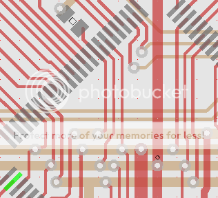
Note the four brown power lines on the back side of the board. The red traces on top provide connections to the power buses using vias. Power lines are routed under the chip, and the breaks offered by them provide room for decoupling caps. Often there will be enough room inside the chip outline and below to route out specialized connections to JTAG and configuration pins, keeping the topside free for IO distribution.
BGA chips require a similar approach. Diagonal power buses on the back will often not provide enough connectivity, and I often sacrifice a number of pins and run power trees on the top level right through them. Some FPGAs feature a ridiculous checkerboard pattern of power and ground pins, but it's not as bad as it looks at first. Here is an early prototype depicting many of the issues facing us.
Here brown represents the back layer with power distribution grid, while blue and red are the top layer connections. Note that I am sacrificing many unnecessary IO pins to provide adequate power to the FPGA. In this prototype I placed the decoupling caps on the back (you can see the faint shadows), explaining the slightly odd shapes of the power lines. I don't think I will ever do that again!
I use the silk layer to liberally mark up the pads. This can be removed later - or just left in place (the fab will eliminate silk from the exposed copper) as no one will see it under the chip. It helped me on one occasion to identify an error.
Routing BGA pins presents a special problem. BGA geometries generally require pads of a certain size, allowing us to route a single trace in between. This restricts us to a maximum of two rows on the top layer and two more (there are no pads but there are the vias) on the bottom. That seems like a steep limitation, but consider that the outer 4 rows of a 484-pin bga yield 288 IO pins - way more than enough for anything I can think of. In practice, the interferance of the power grid will present further limitations.
Inside the square formed by four adjoining FPGA balls, you are given a choice of placing a trace between the balls or placing a via. It's tempting to place vias right under the balls, but don't do it! Vias suck the solder right out of the ball, breaking your connection. Keep the vias right in the center, where they belong.
In the next article I will address the issues of the actual assembly of circuit boards with FPGAs.


- Comments
- Write a Comment Select to add a comment

Are there any more articles in this series?? I can't wait.
Victor, what happened to the rest of the series. This is a topic that I have been thinking about and found your blog entry really good. I was looking for follow-ons (part 2, etc.) and was disappointed there are none (at least that not that I can find).
Dave

Nice article. I've been doing SMD for years, always wondered about BGA's. I appreciate you work!
To post reply to a comment, click on the 'reply' button attached to each comment. To post a new comment (not a reply to a comment) check out the 'Write a Comment' tab at the top of the comments.
Please login (on the right) if you already have an account on this platform.
Otherwise, please use this form to register (free) an join one of the largest online community for Electrical/Embedded/DSP/FPGA/ML engineers:


