


Tolerance Analysis
Today we’re going to talk about tolerance analysis. This is a topic that I have danced around in several previous articles, but never really touched upon in its own right. The closest I’ve come is Margin Call, where I discussed several different techniques of determining design margin, and ran through some calculations to justify that it was safe to allow a certain amount of current through an IRFP260N MOSFET.
Tolerance analysis is used in electronics to determine the amount of variation of some quantity in a circuit design. It could be voltage, or current, or resistance, or amplifier gain, or power, or temperature. When you are designing a circuit, the components that you use will have some nominal value, like a 4.99kΩ resistor, or a 33pF capacitor, or a 1.25V voltage reference, or a 3.3V regulator. That 4.99kΩ resistance is just the nominal value; in reality, the manufacturer claims — and I discussed what this means in an article on datasheets — that the resistance is 4.99kΩ ± 1%, that is, between 4940 and 5040 ohms. Actually, most components have more than one nominal value to characterize their behavior; even a simple resistor has several:
- resistance R
- temperature coefficient of resistance
- thermal resistance in °C / W
- maximum voltage across the resistor
- operating and storage temperature ranges
More complex components like microcontrollers may have hundreds of parameters described in their datasheet.
At any rate, what you care about is not the variation in the component, but the variation of something important in your circuit: some quantity X. Tolerance analysis allows you to combine the variations of component values and determine the variation of X. Here is an example:
Example: Overvoltage Detector, Part 1
I work with digitally-controlled motor drives. It’s usually a good idea to put a hardware overvoltage detector in a motor drive, so that if the voltage across the DC link gets too large, the drive shuts off before components attached to the DC link, like capacitors and transistors, can get damaged. This is important if the drive is operating in regeneration, where the motor is used to provide braking torque to the mechanical load and to convert the resulting energy into electrical form on the DC link, where it has to go somewhere. In an electric bike or a hybrid car, this energy will flow back into a battery. In some large AC mains-connected systems, it may flow back into the power grid. Otherwise, it will cause the DC link voltage to rise, storing some energy in the DC link capacitor, until one of the components fails or the motor drive stops regenerating. (Hint: you don’t want a component to fail; you want the motor drive to stop regenerating.) The control of the motor drive is done through firmware, but you never know when something can go wrong, and that’s why it’s important to have an independent analog sensor that can shut down the gate drives for the power transistors if the DC link voltage gets too high.
So here’s the goal of a hypothetical overvoltage detector for a 24V nominal system:
- Provide a 5V logic output signal that is
HIGHif the DC link voltage \( V_{DC} < V_{OV} \) (normal operation) andLOWif \( V_{DC} \ge V_{OV} \) (overvoltage fault) for some overvoltage threshold \( V_{OV} \). - \( V_{OV} > 30V \) to allow some design margin and avoid false trips
- \( V_{OV} < 35V \) to ensure that capacitors and transistors do not experience voltage overstress.
- The preceding thresholds are for slowly-changing values of \( V_{DC} \). (Instantaneous voltage detection is neither possible nor desirable: all real systems have some kind of noise and parasitic filtering.)
- Under all circumstances, \( V_{DC} \ge 0 \)
- The logic output signal shall detect an overvoltage and produce a
LOWvalue for any voltage step reaching at least 40V in no more than 3μs after the beginning of the step. - Overvoltage spikes between \( V_{OV} - 1.0V \) and 40V, which exceed \( V_{OV} - 1.0V \) for no more than a 100ns pulse out of every 100μs, shall not cause a
LOWvalue. (This sets a lower bound on noise filtering.) - The overvoltage detector will be located in an ambient temperature between -20 °C and +70 °C.
- A 5V ± 5% analog supply is available for signal conditioning circuitry.
For the time being, forget about the dynamic aspects of this circuit (the 40V step detected in no more than 3μs, and the 100ns spikes up to 40V not causing a fault) and focus on the DC accuracy, namely that the circuit should trip somewhere between 30V and 35V.
Let’s also assume, for the time being, that we have a comparator circuit that trips exactly at 2.5V. Then all we need to do is create a voltage divider so that this 2.5V comparator input corresponds to a DC link voltage between 30V and 35V.
We probably want to choose resistors so that their nominal values correspond to the midpoint of our allowable voltage range: that is, 32.5V in produces 2.5V out. That’s a ratio of 13:1, so we could use R1 = 120K and R2 = 10K. Except if you look at the standard 1% resistor values ( (the so-called E96 preferred numbers), you’ll see the closest is R1 = 121K and R2 = 10K, for a ratio of 13.1:1. That gets us to 32.75V in → 2.5V out.
But if these are 1% resistors, then their room-temperature values can vary by as much as ±1%:
- R1 = 121K nominal, 119.79K minimum, 122.21K maximum
- R2 = 10K nominal, 9.9K minimum, 10.1K maximum
If we want to go through a worst-case analysis, the extremes in resistor divider ratio are at minimum R1 and maximum R2, and at minimum R2 and maximum R1:
- R1 = 119.79K, R2 = 10.1K → 12.86 : 1 → 32.15V in : 2.5V out
- R2 = 122.21K, R1 = 9.9K → 13.34 : 1 → 33.36V in : 2.5V out
This gets to be tedious to do by hand, and it can help to use spreadsheets, or analysis in MATLAB / MathCAD / Scilab / Python / Julia / R or whatever your favorite scientific computing environment is:
import numpy as np

def resistor_divider(R1, R2):
    return R2/(R1+R2)

def worst_case_resistor_divider(R1,R2,tol=0.01):
    """
    Calculate worst-case resistor divider ratio
    for R1, R2 +/- tol

    Returns a 3-tuple of nominal, minimum, maximum
    """

    return (resistor_divider(R1,R2),
            resistor_divider(R1*(1-tol),R2*(1+tol)),
            resistor_divider(R1*(1+tol),R2*(1-tol)))

ratios = np.array([1.0/K for K in worst_case_resistor_divider(121.0, 10.0, tol=0.01)])

def print_range(r, title, format='%.3f'):
    rs = sorted(list(r))
    print(("%-10s nom="+format+", min="+format+", max="+format) % (title, rs[1], rs[0], rs[2]))

print_range(ratios, 'ratios:')
print_range(ratios*2.5, 'DC link:')
ratios: nom=13.100, min=12.860, max=13.344 DC link: nom=32.750, min=32.151, max=33.361
I’ve just assumed we were going to use 1% resistors here, because I have experience picking resistors. Even so, it helps to double-check assumptions, so as of this writing, here are the lowest-cost chip resistors for 120K (5%) or 121K (1% or less) in 1000 quantity from Digi-Key. Price is per thousand, so \$2.33 per thousand = \$0.00233 each. (I’m looking up 120K/121K rather than 10K because 10K is a common, dirt-cheap value.)
-
5% 0402: Rohm MCR01MRTJ124, \$2.33
-
5% 0603: KOA Speer RK73B1JTTD124J, \$2.62
-
1% 0402: Stackpole RMCF0402FT120K, \$2.62
-
1% 0603: Stackpole RMCF0603FT120K, \$2.92
-
1% 0805: Rohm MCR10ERTF1203, \$3.45
-
5% 0805: Stackpole RMCF0805JT120K , \$3.50
-
1% 0201: Delta PFR03S-1213-FNH, \$3.74
-
5% 1206: Rohm MCR18ERTJ124, \$4.85
-
5% 0201: Panasonic ERJ-1GNJ124C, \$4.96
-
1% 1206: Stackpole RMCF1206FT120K, \$6.28
-
0.5% 0603: Susumu RR0816P-124-D, \$15.75
-
0.5% 0805: Susumu RR1220P-124-D, \$16.54
-
0.1% 0603: Panasonic ERA-3AEB124V, \$46.73
-
0.1% 0805: Panasonic ERA-6AEB1213V, \$47.12
-
0.1% 0402: Yageo RT0402BRD07121KL, \$66.21
-
0.1% 1206: Yageo RT1206BRD07120KL, \$107.17
The upshot of this is that 1% and 5% chip resistors are now around the same price. You might save a teensy bit with a 5% resistor: \$0.00233 vs \$0.00262 is a difference of \$0.00029 each, or 29 cents more per thousand for 1% resistors. This is much smaller than the cost of a pick-and-place machine to assemble the component on a PCB; it’s harder to get a good estimate of how much that might cost, but if you look at on-line assembly cost calculators for an estimate, you can get an idea. Here’s one which quotes \$0.73 assembly cost per board at 1000 boards, 10 different unique components, 100 SMT parts on one side of the board only; if you increase to 200 SMT parts it’s \$1.28 per board, and 300 SMT parts it’s \$1.76 per board — at that rate, you’re looking at about a half-cent to place each part, so don’t quibble on the difference between resistors that cost 0.233 cents vs. 0.262 cents each. 5% and 1% chip resistors effectively are the same price; you’re going to pay more to have them assembled than to buy them.
So 1% 0603 or 0402 resistors should be your default choice. I’d probably choose 0603 for most boards, since there’s not too much price difference, and on prototypes I can solder those by hand, if I really need to; 0402 and smaller require more skill than I can handle. (DON’T SNEEZE!)
0.5% resistors are a bit more expensive at about 1.5 - 1.7 cents each.
0.1% resistors are still more expensive at 4.6 - 4.7 cents each, but that’s not too bad if you need the accuracy.
(The 1% and 5% resistors are thick-film chip resistors; the 0.5% and 0.1% resistors are thin-film. For the most part this is just an internal construction detail, but more on this subject in a bit.)
At any rate, we figured out that we could use 1% resistors and have our 2.5V threshold at the comparator equivalent to something between 32.15V and 33.36V at the DC link.
Are we done yet?
No, because there are a bunch of other things that determine resistor values. Let’s look at the datasheets for KOA Speer RK73H (\$4.08 per thousand for 0603 1% RK73H1JTTD1213F) and Panasonic ERJ (\$8.72 per thousand for 0603 1% ERJ-3EKF1213V):
Both have a temperature coefficient of ±100ppm/°C. Our ambient spec of -20°C to +70°C deviates from room temperature by 45°C. (Let’s assume the board doesn’t heat up significantly.) That will add another 4500ppm = 0.45%.
Then there are all these gotchas where the resistance can change by 0.5% - 3% from overload, soldering heat, rapid change in temperature, moisture, endurance at 70°C, or high temperature exposure. The more serious one is soldering heat.

Panasonic:

Yes, that’s right, your resistors meet their advertised 1% specs when they aren’t connected to anything; if you actually want to solder them to a board, their resistance value will change. Some of you are reading this and thinking, “Sure, of course the resistance will change, it’s some function of temperature R(T).” That implies reversible resistance change, back to its original value, after the part cools down. But the resistance may also undergo irreversible change. Some of that is probably due to slight physical or chemical changes in the resistor caused by heating and cooling, and some of it is due to the strain placed on the part by the solder solidifying. I found a few documents on this subject. From a Vishay application note titled “Reading Between the Lines in Resistor Datasheets”
The end customer must also evaluate whether a tolerance offered by a manufacturer is really practical. For example, some surface mount thin film chip resistors are offered in very tight tolerances for very low resistance values. That’s impressive on the datasheet but not compatible with assembly processes. As these resistors are mounted on the board there is a resistance change due to solder heat. The solder terminations melt, flow, and re-solidify with changed resistance values. For low-value resistors the amount of resistance change is much greater than the specified tolerance. Having paid a premium price for an impractically tight tolerance, the customer ends up with looser-tolerance resistors once they’re assembled on the PCB.
One study, Capacitors and Resistors Mounting Guide Survey Based on Commercial Manufacturers’ Public Documents, mentions sulfur contamination:
Sulphur contamination is mainly associated with use and reliability of thick-film chip resistor with Ag-system as inner termination. The silver in the inner termination is very susceptible to contamination via sulphur which produces silver sulphide in chip resistors. Silver is so susceptible to combination with sulphur that the sulphur diffuses through the outer termination layers to the inner termination forming silver sulphide. Silver sulphide unfortunately makes the termination material nonconductive and effectively raises the resistance value until it is essentially open circuit. The reaction velocity in this case is influenced by sulphur gas density, temperature and humidity greatly. This process can be initiated or inhibited already by heat-stress while mounting.
…
Inert gas atmosphere mounting (as mentioned in this chapter above) can be recommended as a prevention measure to suppress the sulphide contamination issues.
As for the effects of strain, one concern is piezoresistivity: you can read another Vishay application note titled “Mechanical Stress and Deformation of SMT Components During Temperature Cycling and PCB Bending”. No good sound bites in this one, other than the in conclusion:
The piezoresistive effect can cause significant resistance changes to thick film chip resistors, especially when the PCB bends, temperature changes occur, or the components experience stress when they are embedded or molded. The component’s TCR will be also affected.
These effects are not seen in thin metal film chip resistors.
So that’s another reason why the SMT resistors that are better than 1% tolerance are thin-film. This affects SMT more than through-hole parts, because there’s not much strain relief for chip components; through-hole parts at least have leads to allow the part to avoid mechanical stress when the board flexes a little bit. Neither of the resistor datasheets I showed above, however, mentions the effect of strain on resistance.
La la la la la, let’s just pretend we didn’t hear all that, and we have ± 1.45% resistance tolerance due to part variation and temperature coefficients.
ratios = np.array([1.0/K for K in worst_case_resistor_divider(10.0, 121.0, tol=0.0145)])
print_range(ratios, 'ratios:')
print_range(ratios*2.5, 'DC link:')
ratios:    nom=13.100, min=12.754, max=13.456
DC link:   nom=32.750, min=31.885, max=33.640
Now we’re looking at 31.89V to 33.64V. Still within our spec of 30-35V for \( V_{OV} \). Are we done yet?
No — we need the rest of the circuit, it’s not just a voltage divider.
But before we go there, let’s look at how the resistor tolerance affects the voltage divider ratio.
import matplotlib.pyplot as plt
%matplotlib inline

alpha = np.arange(0.001, 1 + 1e-12, 0.001)
Rtotal = 10e-3   # this doesn't matter
R1 = alpha*Rtotal
R2 = (1-alpha)*Rtotal
for whichfig, ytext, ysym in [(1,'Ratio','\\rho'),
                              (2,'Sensitivity','S')]:
    fig = plt.figure()
    ax = fig.add_subplot(1,1,1)
    for tol in [0.1, 0.05, 0.01]:
        r_nominal, r_min, r_max = worst_case_resistor_divider(R1, R2, tol)
        S = np.maximum(r_nominal-r_min, r_max-r_nominal) / tol
        y = S if whichfig == 1 else S/alpha
        ax.plot(alpha, y, label='$\\delta = $%.1f%%' % (tol*100))
    ax.grid(True)
    ax.legend(loc='best', fontsize=11, labelspacing = 0)
    ax.set_xlabel('$\\alpha$',fontsize=14)
    ax.set_ylabel('$%s$' % ysym,fontsize=14)
    nt = np.arange(11)
    xt = nt * 0.1
    ax.set_xticks(xt)
    ax.set_title(('%s $%s(\\alpha, \\delta) = (V - \\bar{V})/(%s\\delta\\cdot V_{\\rm in})$\n'
                +'$R_1=\\alpha R, R_2=(1-\\alpha R), V = \\alpha V_{\\rm in}$')
                 % (ytext, ysym, '' if whichfig == 1 else '\\alpha \\cdot'));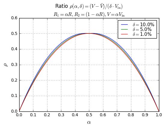
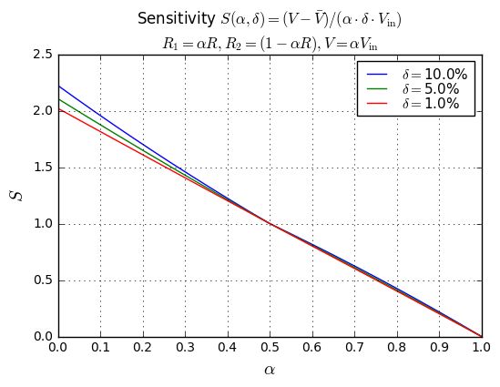
OK, what are we looking at? The top graph, \( \rho(\alpha, \delta) \) is the ratio of the voltage divider error to the resistor tolerance, where \( \alpha = \) the nominal voltage divider ratio, and \( \delta \) is the resistor tolerance. The bottom graph, \( S(\alpha, \delta) \) is the sensitivity of the voltage divider output; we just divide by the nominal voltage divider ratio, so \( S = \frac{\rho}{\alpha} \).
Here are three concrete examples:
-
\( R_1 = R_2 = R \) and \( \delta = \) 1%. Then \( \alpha = R_1/(R_1+R_2) = 0.5 \) and the output can vary from 0.99/(0.99+1.01) = 0.495 to 1.01/(1.01+0.99) = 0.505. This is a ±0.005 output error, and if we divide by \( \delta = 0.01 \) we get \( \rho = 0.5 \) and then \( S = \rho / \alpha = 1. \)
-
\( R_1 = R, R_2 = 4R \) and \( \delta = \) 1%. Then \( \alpha = R/5R = 0.2 \) and the output can vary from 0.99/(0.99+4.04) = 0.1968 to 1.01/(1.01+3.96) = 0.2032. This is a ±0.0032 output error, and if we divide by \( \delta = 0.01 \) we get \( \rho = 0.32 \) and then \( S = \rho / \alpha = 1.6. \)
-
\( R_1 = 4R, R_2 = R \) and \( \delta = \) 1%. Then \( \alpha = 4R/5R = 0.8 \) and the output can vary from 3.96/(3.96+1.01) = 0.7968 to 4.04/(4.04+0.99) = 0.8032. This is a ±0.0032 output error, and if we divide by \( \delta = 0.01 \) we get \( \rho = 0.32 \) and then \( S = \rho / \alpha = 0.4. \)
Some important takeaways are:
- The ratio \( \rho \approx 2\alpha(1-\alpha) \) and sensitivity \( S \approx 2(1-\alpha) \).
- Absolute error in voltage divider output is symmetrical with \( \alpha \) and reaches a maximum for \( \alpha=0.5 \) and is very low for \( \alpha \) near 0 or 1.
- Sensitivity of voltage divider output for \( \alpha << 1 \) is approximately \( S=2 \). If I am dividing down a much higher voltage to a lower voltage, this means if I use 1% resistors I can expect about 2% gain error, or if I use 0.1% resistors I can expect about 0.2% gain error.
- Sensitivity of voltage divider output for \( \beta << 1 \) where \( \beta = 1-\alpha \) is approximately \( S=2\beta \). This means if I want a voltage divider ratio that is very close to 1, and I use 1% resistors I can expect a much lower gain error. In one of my earlier articles on Thevenin equivalents I used the example of R1 = 2.10kΩ, R2 = 49.9Ω where \( \alpha = 0.9768, \beta = 0.0232 \), and that means for 1% resistors I can expect a gain error of only about 0.0464%.
ratios = np.array([1.0/K for K in worst_case_resistor_divider(2100, 49.9, tol=0.01)])
print_range(ratios, "ratios", '%.5f')
print "sensitivity S", ratios[1:3] - ratios[0]
ratios     nom=1.02376, min=1.02329, max=1.02424
sensitivity S [ 0.00048004 -0.00047053]
Overvoltage Detector, Part 2: The Other Stuff at DC
Here’s the whole circuit we’re going to be looking at:

Selecting 2.5V Voltage References
First we need a 2.5V source, so we can compare the output of our voltage divider to it.
TL431
In theory, I like the TL431 type of shunt voltage reference. It’s a three-terminal device that’s kind of like a precision transistor: if the reference terminal is less than its 2.5V threshold, it does not conduct from cathode to anode; if it’s greater than its 2.5V threshold, it does conduct.
TL431s are cheap and ubiquitous. You want a 0.5%-tolerance 2.5V reference for less than 10 cents in quantity 1000? You got it. The Diodes Inc. AN431 is available in 0.5% grade from Digi-Key for about 7 cents in quantity 1000. This is pin- and function-compatible with the TL431. (Mess up the pinout? There’s the AS431, same price, which swaps ref and cathode pins, compatible with the TL432.)
The only downside is that its voltage accuracy is specified at 10mA, so that’s kind of a power hog. You can run it down as low as 1mA, but then you have to use the specification for dynamic impedance, \( Z_{KA} \) to figure out how much the voltage changes at 1mA. For the AN431, it’s a maximum of 0.5Ω, so for a change from 10mA down to 1mA (ΔI of -9mA), the voltage could drop by as much as 4.5mV, which adds another 0.18% to the effective accuracy.
Low-current TL431
The next step up from those are the ON Semiconductor NCP431B which you can buy from Digi-Key at 9.9 cents each in quantity 1000. These work down to at least 60μA, and their voltage accuracy is specified at 1mA. The dynamic impedance \( Z_{KA} \) is specified between 1mA and 100mA (same 0.5Ω maximum), but there is no spec for 60μA to 1mA — they do show a figure 36 (“Knee of Reference”) claiming a typical 4.5A/V = 0.22Ω, and you could decide to use the 0.5Ω maximum value and double it for good measure: 1 ohm times (100μA - 1mA) = 0.9mV, which is less than 0.04% of 2.5V. But there’s no spec, so how can you possibly know whether you can trust the voltage accuracy at those low currents? You could have a part that regulated to 2.45V at 100μA and it would meet the specification but represent a 50mV error from nominal.
Diodes Inc has the AP431 for 8.6 cents (quantity 1000) from Digi-Key with similar specs: ±0.5% at 1mA, works down to 100μA cathode current, dynamic impedance \( Z_{KA} \) < 0.3Ω from 1mA to 100mA. But nothing useful for determining voltage accuracy below 1mA.
Diodes Inc also has the ZR431 which it inherited from Zetex, specified at 10mA and no specs below 10mA.
TI has the similar ATL431LI for 17 cents (qty 1000) from Digi-Key, ±0.5% at 1mA, works down to 100μA cathode current, dynamic impedance \( Z_{KA} \) < 0.65Ω from 1mA to 15mA, and nothing about voltage accuracy below 1mA.
These guys are either copying each other’s collective blunders, or there’s a conspiracy, a kind of mini-Phoebus cartel when it comes to specifying voltage accuracy below 1mA. Sigh. My guess is that it was Zetex’s fault for poor specsmanship of the ZR431, and then everybody just copied the general form of the datasheet, without bothering to make any claims about low-current voltage accuracy.
LM4040 / LM4041
The next step up are the LM4040 and LM4041 voltage references; these have specified voltage accuracy at 100μA operation, and are available from a number of manufacturers. The LM4040 is a fixed voltage reference, and the LM4041 is an adjustable reference based on a 1.23V bandgap voltage, kind of an upside-down TL431. For precision circuits, unless you need the adjustability, the LM4040 is a better choice; otherwise, you’ll need to add your own resistor divider which will raise the effective tolerance. For the LM4040, if you get the A grade version, it’s 0.1% accuracy, but you’ll pay extra for that. Here are some options for the C grade (0.5% accuracy), prices from Digi-Key at 1000 piece quantity:
TI also has the TL4050 which has some nice specs but it’s more expensive.
Series references
Finally, if you are working with micropower designs and you really need to guarantee low current, or you need to minimize parts count, there are series references which will give you a buffered voltage reference, like the ones listed below, but you’ll pay more for them, typically in the 50-60 cent range in 1000 quantity.
Designing with 2.5V shunt references
I’m going to stick with the ON Semi NCP431B, and just use it at 1mA — although I still think it’s a tragedy that you can’t rely on the voltage spec below 1mA.
For the NCP431BI, the voltage specification at 1mA current over its temperature range is 2.4775V to 2.5125V.
Our 5V ± 5% supply can go as low as 4.75V. We’ll use a 2.00kΩ shunt resistor with it to guarantee a minimum cathode current of (4.75V - 2.5125V) / (2.00kΩ × 1.0145) = 1.103mA. (Remember: the factor of 1.0145 comes from the 1% resistor range on top of the 4500ppm swing due to 100ppm/°C tempco and ±45°C swing. This is slightly above the 1mA voltage specification, and leaves 103μA above spec, which is much more than the max gate current of 190nA.)
On the other side of the tolerance ranges, we could have as much as 5.25V, with a cathode current of up to (5.25 - 2.4775) / (2.00kΩ × 0.9855) = 1.41mA. The specification on dynamic impedance \( Z_{KA} \) < 0.5Ω tells us we might see as much as (1.41 - 1mA) * 0.5Ω = 0.205mV increase due to worst-case cathode current tolerance, making our overall voltage reference range:
- 2.500V nominal
- 2.5127V maximum (2.5125V + 0.205mV)
- 2.4775V minimum
Selecting comparators
We also need a comparator. The important system requirements are that we want one that can be powered from 5V in ambient temperatures of -20 to +70°C, has a short enough response time, and doesn’t introduce much voltage error. Our system requirement of at most 5 microsecond response time for a 40V 1μs pulse means, at first glance, that we’ll probably need a fast response, say around 1μs or less, but there are some factors that work both for and against us to meet the system requirement.
Aside from that, it’s a matter of good judgment and frugality. The most inexpensive comparators, by far, are of the LM393 variety. Digi-Key price in 1000 quantity is about the same; the lowest is the ON Semi LM393DR2GH in a SOIC-8 package, at about 8.4 cents. Others from TI, ST, and Diodes Inc. are in the 8.5 - 10 cent range.
They are so cheap that you cannot buy a single comparator for less money; the LM393 is a dual comparator, with open-collector output, and if you’re not going to use the second comparator, you have to read the fine print in the datasheet, which says that unused pins should be grounded.
There are a couple of important specs in the LM393 datasheet to note:
-
Offset voltage. This is ± 5mV max at 25°C and ± 9mV max over the full temperature range; this effectively adds to the 2.5V reference tolerance; ± 9mV is 0.36% of 2.5V
-
Response time. This is typically 1.3μs for a 100mV step change with 5mV overdrive, which means that to turn the comparator from output high to output low, we start with Vin- 95mV below Vin+, and then increase Vin- to 5mV above Vin+. Think of this device as a balance scale: if the two inputs are nearly equal, then the output can change slowly, whereas if they are different enough, the balance will tip quickly to note which is greater. Comparator datasheets will usually have graphs showing typical response time vs. overdrive level. The ON Semi LM393 does not, and this is one reason it may be better to pick another part. Here are the response time graphs from the TI LM393 datasheet — I prefer the original from National Semiconductor before they were acquired by TI, but unfortunately TI hasn’t maintained earlier variants, so we’re stuck with the more confusing TIified version:


You will note that the output transition from high-to-low is faster than the low-to-high transition. The reason for this may be clearer if we look at the simplified equivalent circuit — which is part of why these parts are so cheap. They’re simple!

All we really have here is a Darlington bipolar differential pair (Q1-Q4), loaded down by a current mirror (Q5 and Q6), with an open-collector output stage (Q7 and Q8).
-
When the positive input is greater than the negative output, then more than half of the 100μA current source flows through Q3 than Q2; Q2, Q5, and Q6 have the same current flowing through them, so more current flows through Q3 than Q6, and that turns Q7 on which turns Q8 off, and the output is open-collector.
-
When the negative input is greater than the positive output, the reverse is true: more than half of the 100μA current source flows through Q2 than Q3, which means more current flows through Q6 than Q3, and that turns Q7 off which turns Q8 on, and the output is pulled low.
The reason the high → low transition is faster than the low → high transition is because the output transistor Q8 has storage time to come out of saturation. It’s a bit puzzling why National didn’t make a version of the LM393 comparator with a Baker clamp on the output transistor to speed up this time. It’s also too bad the LM393 doesn’t have separate specs for turn-on and turn-off transition times — although since they’re typical rather than maximum specs, you might as well just use the graphs for information instead. (Or use a part like the ON Semi TL331 which lists typical values in the spec tables.)
Anyway, this is important because we have a system requirement to detect overvoltage and transition from high-to-low within a bounded time, but no time requirement to transition in the other direction. So in our particular application, we care about the high-to-low response time.
-
Other specs of importance to ensure it will work for our application are:
-
Common-mode voltage range: down to zero (because of the PNP input stage), up to Vcc - 2.0V over the full temperature range (Vcc - 1.5V at 25°C) — we need this to work at 2.5V input, and Vcc can be as low as 4.75V, so we can support an input voltage range up to 4.75 - 2.0 = 2.75V. That represents a voltage margin of a quarter-volt (2.75V - 2.5V).
-
Input bias current (400nA max) and input offset current (150nA max): The LM393 is a bipolar device, not CMOS, so the inputs are not perfectly high-impedance. Input bias current is the current flowing through each input. Input offset current is the difference between the two input bias currents. If your input sources have low enough impedance, you can ignore input offset current and just analyze the input bias currents; otherwise, you can try to match source impedances so the voltage drop across your source impedances cancel to some extent. An upper bound for voltage error in either case is \( \Delta R I_{\textrm{bias}} + RI_{\textrm{ofs}}. \)
In this application, we’re using R1 = 10K, R2 = 121K, so the source impedance is 10K || 121K = 9.24K, and the voltage error at the comparator input is 9.24K × a maximum of 400nA = 3.7mV. This is small (0.15%) but not zero. It’s not hard to match the input impedances to 10K || 121K. In this case, the worst-case voltage error at the comparator inputs is \( \Delta R I_{\textrm{bias}} + RI_{\textrm{ofs}} \) = 9.24K × 0.02 × 400nA + 9.24K × 150nA = 1.46mV.
-
Operating temperature range: Here we’re in trouble. The LM393 is rated for an operating range of 0 - 70°C, but we need a circuit that works down to -20°C.
C, I, M (Temperature ratings)
For those of us engineers of a certain age, the letters CIM mean something:
- C = commercial (0 - 70°C)
- I = industrial (“cold” - 85°C) where “cold” varied by manufacturer: for example, -40°C for TI and Motorola, -25°C for National Semiconductor
- M = military (-55°C - 125°C), usually in ceramic rather than plastic packages
TI used the CIM lettering system, sometimes CIME or CIMQ; see for example the TLC272 and TLC393 — the TLC393 datasheet states
The TLC393C is characterized for operation over the commercial temperature range of TA = 0°C to 70°C. The TLC393I is characterized for operation over the extended industrial temperature range of TA = −40°C to 85°C. The TLC393Q is characterized for operation over the full automotive temperature range of TA = −40°C to 125°C. The TLC193M and TLC393M are characterized for operation over the full military temperature range of TA = −55°C to 125°C.
“E” (extended) was sometimes -40°C to +125°C. Presumably coverage of the -55°C to -40°C range was difficult to design and test, and aside from military and aerospace usage, it is not a frequent need in circuit design.
ON Semiconductor appears to use something similar, at least for the NCP431:
- C = 0 to +70°C
- I = -40 to +85°C
- V = -40 to +125°C
National Semiconductor used the part number to indicate temperature range: for example, the LM393 datasheet includes the LM193 (military temp range), LM293 (industrial), and LM393 (commercial), so the LM3xx series was commercial, LM2xx was industrial, and LM1xx was military.
Other manufacturers like Burr-Brown and Linear Technology just tended to design everything for -40°C to +85°C by default, sometimes with military-grade variants to cover the -55°C to +125°C range. This is now the more typical behavior for more recent devices from most manufacturers. Instead of seeing 3 or 4 temperature grades, new devices may have only 1 or 2, with different specs covering the 0 to 70 or -40 to +85 ranges.
LM293
At any rate, to cover our -20°C to +70°C range, we need the LM293, not the LM393. (And for the reference, we’ll need the NCP431BI.) This isn’t a big deal nowadays (it was more significant 10-20 years ago; the industrial and military range devices were more expensive and less common): Digi-Key sells the LM293ADR for just under 10 cents at 1000 quantity.
Better comparators
We could also use the TI LM393B or LM2903B comparators, which are basically LM293 with better specs in almost every area (it’s part of the same datasheet):
- temperature range (LM393B = -40°C to +85°C; LM2903B = -40°C to +125° C)
- offset voltage: 2.5mV at 25°C, 4mV over temperature range
- input bias and offset current: 50nA max input bias current, 25nA max input offset current (vs. 400nA, 150nA for LM193/293/393)
- supply voltage: 3-36V operating, as compared to 2-30V for the LM193/293/393 (note that we have to give up ultra-low supply voltage, but that’s ok in our application)
- response time: 1μs typ. (vs. 1.3μs for LM393)
- quiescent current: 800μA worst-case (vs. 2.5mA for the LM393)
- output low voltage: 550mV max at 4mA sink (vs 700mV max at 4mA sink for the LM393)
Common-mode input voltage is the same.
Cost from Digi-Key in 1000 quantity is about 9.4 cents for the LM393B and 9.0 cents for the LM2903B. Since the LM2903B has a wider temperature range for the same specs, and is slightly cheaper — an example of price inversion! — we’ll use the LM2903B.
The other kind of specs that are available in more expensive comparators include:
- lower offset voltage (rare)
- push-pull output instead of open-collector
- rail-to-rail input
- CMOS input for supporting high-impedance applications
- faster response
- micropower
- built-in voltage reference
We don’t need them for our application — although a built-in voltage reference would be cost-effective if we could find a part that has about the same total price as the 2.5V reference and the comparator — but you should know about them in case you need those sorts of things. Just for a couple of examples, you can look at the ON Semi NCS2250 or TI LMV762 or TI TLV3011 or Maxim MAX40002. The least-expensive comparator with built-in voltage reference that I could find is the Microchip MCP65R41T-2402E for 33 cents at Digi-Key, and that costs more than the voltage reference and comparator we picked; for applications that are size-constrained, this kind of device might be appropriate.
Hysteresis
To help the comparator switch quickly and avoid noise sensitivity when its input is around the voltage threshold, we need to add some positive feedback. We don’t need much; only a few millivolts is sufficient. The easiest way to do this is put a little resistance between our 2.5V source and the comparator’s + input. Perhaps 1kΩ. Then add 1MΩ from the comparator’s output to the + input. This will form a 1001:1 voltage divider, adding approximately 2.5mV if the output is at 5V, and subtracting approximately 2.5mV if the output is at 0V.
Now, in reality we don’t reach either 5V or 0V output: at the top end, it depends on the pullup resistance of our open-collector circuit in series with the 1MΩ resistor — the LM2903B’s specs are listed with a 5.1kΩ pullup resistor, so instead of a 1001:1 voltage divider, we’ll have effectively a 1006:1 voltage divider, adding at least roughly 2.49mV hysteresis to the threshold to turn the comparator output low.
If you really want to incorporate the effects of resistor tolerance over temperature range, then run the numbers for (1MΩ+5.1kΩ)×(1±0.0145) and 1kΩ × (1∓0.0145):
hyst = np.array([K*2500 for K in worst_case_resistor_divider(1005.1, 1, tol=0.0145)])

print_range(hyst, 'hysteresis (mV):')
hysteresis (mV): nom=2.485, min=2.414, max=2.558
That’s only about ± 72μV, which is really small, and represents less than 0.003% error compared to the 2.5V threshold, which is insignificant compared to the dominant sources of error — namely the 0.5% accuracy of the reference itself.
At the turn-off point, where output is transitioning from low to high, the LM2903B has a max spec of output voltage low at 0.55V with current of 4mA or less; the 1001:1 voltage divider will give us roughly (2.5 - 0.55)/1001, subtracting at least roughly 1.95mV hysteresis to the threshold to turn the comparator output high.
Since the effect of resistance tolerance on turn-off hysteresis is small and not very critical to our application, we’ll ignore it.
Designing with the LM2903B
Here are the error sources for the LM2903B:
- Offset voltage: 4mV max over temperature
- Input bias current: 50nA max over temperature — with our 121K / 10K input voltage divider on the negative input, this leads to additional effective offset voltage of at most 50nA × (121K || 10K) = 0.46mV, which is low enough that we don’t have to care about matching input resistance on the posiive input, as long as its source resistance is smaller.
That’s a total input voltage offset error of 4.46mV.
Putting It All Together
Okay, so here’s our full circuit design:
- R1 = 121kΩ
- R2 = 10.0kΩ
- R3 = 2.00kΩ
- R4 = 1.00kΩ
- R5 = 1.00MΩ
- R6 = 5.1kΩ
- U1 = 1/2 LM2903B
- U2 = NCP431B
- C1 = 56pF
- C2 = 100pF
We’ll discuss the reasons for selecting these capacitor values in the next section.
- R1 and R2 set the voltage divider ratio for comparison against the voltage reference producing Vthresh = 2.5V.
- R3 sets the shunt current into the NCP431B to at least 1.1mA worst-case, so it is definitely more than the 1mA level at which the voltage reference is specified
- R4 and R5 set the approximate hysteresis level = ≈ R4/R5 × (Vout - Vthresh)
- R6 sets pulldown current when the output is low; this value just matches the 5.1kΩ value cited in the datasheet. (if the value is too low, then it increases current consumption and may violate the comparator specifications for output voltage level, which are for 4mA or less; if the value is too high, then the switching speed will suffer and, in the extreme, may not reach a valid logic high)
We can now determine the worst-case DC thresholds for comparator output switching, by combining the tolerance analysis we completed earlier:
- Resistor divider ratio R1/R2: nominal=13.100, minimum=12.754, maximum=13.456
- Voltage reference: nominal=2.500V, minimum=2.4775V, maximum=2.5127V
- Comparator:
- Total input voltage error (including input offset voltage + input bias current) is at most 4.46mV
- Hysteresis to turn output low: add ≈ 2.49mV to the + input (this has a roughly ±3% variation due to resistor tolerances, but that error is down around 72μV)
- Hysteresis to turn output high: subtract between 1.95mV and 2.5mV
The input voltage levels are therefore:
Turn-on: (no overvoltage → overvoltage)
- 32.783V nominal = 13.1 × (2.500V + 2.49mV)
- 31.572V minimum = 12.754 × (2.4775V − 4.46mV + 2.49mV − 72μV)
- 33.905V maximum = 13.456 × (2.5127V + 4.46mV + 2.49mV + 72μV)
Overall tolerance is about 3.4-3.7%, and consists approximately of:
- ±2.7% tolerance from resistor divider
- −0.9%, +0.5% tolerance from voltage reference
- ± 0.18% tolerance from input voltage error of comparator
Turn-off: (overvoltage → no overvoltage)
- 32.717V nominal = 13.1 × (2.500V − 2.5mV)
- 31.508V minimum = 12.754 × (2.4775V − 4.46mV − 2.5mV − 72μV)
- 33.846V maximum = 13.456 × (2.5127V + 4.46mV − 1.95mV + 72μV)
Hysteresis:
- 65mV nominal = 13.1 × (2.49mV + 2.5mV)
- 57mV minimum = 12.754 × (2.49mV − 72μV + 1.95mV)
- 67mV maximum = 13.456 × (2.49mV + 72μV + 2.5mV)
These levels are well within our 30V - 35V requirement for DC voltage trip threshold.
Overvoltage Detector, Part 3: Dynamics
Electronics don’t respond instantly to changes, so we have to take into account the dynamics of our input and our circuit. This involves the choice of capacitor values and possibly the comparator.
NCP431B Bypassing
Capacitor C2 is just a bypass capacitor for the NCP431B, used to dampen high-frequency noise. Most of the TL431-style shunt references have a kind of anti-Goldilocks behavior, where the reference is stable when the parallel capacitance is small or large, but it may oscillate when the capacitance is just right. Figure 19 from the NCP431B datasheet shows this:
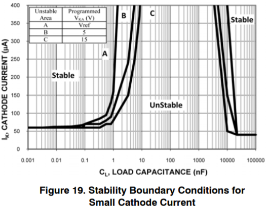
Since we’re not using it with a voltage divider to bump up the cathode-to-anode voltage \( V_{KA} \) beyond the 2.5V value, we’re stuck with curve A, which says that the parallel capacitance should either be below about 1nF or above 10μF for cathode currents above 400μA. (Figure 18 shows cathode currents in the 0-140mA range, but it’s essentially impossible to read the limits for 1mA cathode current — which is rather unfortunate, since the voltage spec for this part is at 1mA; neither of Figures 18 or 19 are very helpful for currents in the 1-10mA range.)
At any rate, we’ll choose C2 = 100pF, which is low enough to stay below the lower capacitance limit, but high enough to keep the output low-impedance at high frequencies. Just as a double-check: at f=10MHz, the capacitor impedance is \( Z=1/j2\pi fC \rightarrow \left|Z\right| = 159\Omega \). Figure 13 in the datasheet shows typical dynamic output impedance vs. frequency, with about 0.5Ω at 1MHz and about 4Ω at 10MHz, so a 100pF isn’t going to change that much, and even a 1000pF at the edge of stability would still have higher impedance than the curve in Figure 13. But passive components are cheap insurance; it’s hard to be 100% certain that the silicon will dampen noise without some kind of capacitance hanging on the output.
Other devices, such as the LM4040, are designed to be stable with any capacitive load, but you’ll generally pay more.
Comparator response time
OK, as far as the comparator response time goes, we have to look at the LM2903B datasheet. Figures 30, 31, 36, and 37 help characterize typical comparator response time as a function of overdrive.
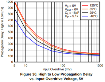


Now, we have a response time requirement for a 40V input transient. This is way above the DC threshold for our comparator circuit. When tolerances are at their worst, the input voltage divider is 13.456 : 1, and the maximum threshold for the circuit is 33.905V, or 2.520V at the comparator “−” input. If we have an input voltage of just over 33.905V, it will trip the comparator eventually, but it might take a long time. To ensure a faster response, we need to exceed this worst-case comparator threshold by some nominal amount: this is the overdrive level. The datasheet specifies typical response time at 5mV or greater. At 5mV, the typical propagation delay is 1000ns.
(Interestingly, while the high-to-low output delay can be lower than low-to-high, it looks like for very low overdrive levels, the low-to-high output delay is lower.)
I’m going to read these figures off the +85°C graph of Figure 30:
- 1000ns for 5mV
- 620ns for 10mV
- 410ns for 20mV
- 260ns for 50mV
- 200ns for 100mV
And here’s how we’ll utilize the overdrive curve: I’ll pick a couple of capacitor values for C1, and we’ll look at the RC relaxation curves for a step input from 0V → 40V. (which yields 2.973V at the output of the voltage divider when it is at its worst-case value of 13.456 : 1)
With this worst-case voltage divider, the Thevenin-equivalent resistance is (121K + 1.45%) || (10K − 1.45%) = 9.12kΩ. Let’s see what happens if we use C1 = 47pF.
def scale_formatter(K):
    def f(value, tick_number):
        return value * K
    return plt.FuncFormatter(f)

def show_comparator_response(R1nom, R2nom, C, Rtol, Ctol):
    tmax = 4e-6
    t = np.arange(-0.1,1,0.001) * tmax
    ovtresp_comparator=np.array([(5e-3,1000e-9),
                      (10e-3,620e-9),
                      (20e-3,410e-9),
                      (50e-3,260e-9),
                      (100e-3,200e-9),
                      (200e-3,165e-9),
                      (300e-3,155e-9),
                      (400e-3,150e-9),
    #                  (500e-3,145e-9),
    #                  (1000e-3,135e-9)
                                ])
    ov_comp = ovtresp_comparator[:,0]
    t_comp = ovtresp_comparator[:,1]
    tresp_requirement = 3e-6
    Vthresh_max = 2.520
    R1 = R1nom*(1+Rtol)
    R2 = R2nom*(1-Rtol)
    Rth = 1.0/(1.0/R1 + 1.0/R2)
    RC = Rth*C*(1+Ctol)
    K = R2 / (R1+R2)
    # Driving signal
    Vin_end = 40
    y_end = Vin_end*K
    u = (t >= 0) * y_end
    y = (t >= 0) * y_end * (1-np.exp(-t/RC))
    # time for RC filter to reach a particular overdrive level above Vthresh_max
    y_ov = Vthresh_max+ov_comp
    t_ov = -RC*np.log((y_ov-y_end)/(0-y_end))

    fig = plt.figure(figsize=(7,4))
    ax = fig.add_subplot(1,1,1)
    ax.plot(t,u)
    ax.plot(t,y)

    xlim = [-0.1*tmax, tmax]
    ylim = [0,3]
    ax.plot(xlim, [Vthresh_max, Vthresh_max],color='red',dashes=[3,2],linewidth=0.8)
    ax.plot([tresp_requirement, tresp_requirement], ylim, color='red',dashes=[3,2],linewidth=0.8)
    ax.plot(t_ov+t_comp, y_ov, '-', color='red')
    tresp_min = (t_ov+t_comp).min()
    #for t1,t2,y1 in zip(t_ov,t_comp,ov_comp):
    #    print t1*1e6,t2*1e6,y1
    ax.fill_betweenx(y_ov, t_ov, t_ov+t_comp, color='red', alpha=0.25)
    ax.xaxis.set_major_formatter(scale_formatter(1e6))
    ax.set_xlabel(u'time (\u00b5s)')
    ax.set_xlim(xlim)
    ax.grid(True)
    ax.set_ylabel(u'Voltage (V)')

    ax.annotate(u"$t_\\min = $%.2f\u00b5s" % (tresp_min*1e6),
                  xy=(tresp_min, Vthresh_max), xycoords='data',
                  xytext=(0,-50), textcoords='offset points',
                  size=14, va="center", ha="center",
                  bbox=dict(boxstyle="round", fc="w"),
                  arrowprops=dict(arrowstyle="-|>",
                                  connectionstyle="arc3",
                                  shrinkA=0
                                 ),
                  )

    ax.set_title(('Comparator response to RC filter; steady-state voltage = %.2fV (%.3fV @comp)\n'
                  +'thresh voltage = %.2fV (%.3fV @comp), R1=%.1fK+%.0f%%, R2=%.1fK-%.0f%%, C=%.0fpF+%.0f%%')
                 % (Vin_end, y_end, Vthresh_max/K, Vthresh_max,
                    R1nom/1e3, Rtol*100, R2nom/1e3, Rtol*100, C*1e12, Ctol*100),
                fontsize=9)

show_comparator_response(121e3, 10e3, 47e-12, 0.0145, 0.05)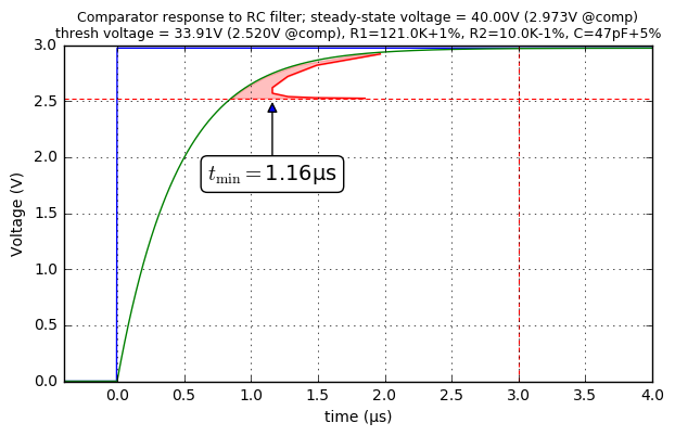
Here a little explanation is needed.
- The blue step is the divided-down voltage from an input step from 0V to 40V at the DC link, with no capacitive load.
- The green curve is the voltage at the comparator “−” input, caused by RC filtering.
- The horizontal dashed line at 2.52V represents the worst-case highest voltage at the “−” input that would trip the comparator. (Nominal is at 2.5V + 2.49mV = 2.502V, remember?)
- The vertical dashed line at 3μs represents our time limit to respond to this step.
- The red curve is the typical comparator response time added to the green curve.
For that red curve, imagine a few cases:
-
that the green curve came up to the comparator threshold of 2.52V and stayed there. No overdrive. This takes about 0.85μs, but the comparator may take forever to switch, because there is no overdrive. (No overdrive = takes forever.)
-
that the green curve came up to 2.525mV, and then stopped increasing. That represents a 5mV overdrive, also at around t=0.85μs after the input step, and it would typically take another microsecond for the comparator output to switch with 5mV overdrive, for a total of about 1.85μs
-
that the green curve came up to 2.92V and stayed there, with 400mV overdrive. This time, with 400mV overdrive it only takes 150ns for the comparator to switch, but the green curve took 1.82μs to get to that point, for a total of 1.97μs. (High overdrive = comparator switches quickly, but capacitor takes forever to get to that point.)
-
finally, there is a sweet spot at around 100mV overdrive, which the green curve reaches at around 0.96μs, and with 100mV overdrive the typical response time is 200ns, for a total of 1.16μs.
So we can expect the comparator to switch output low roughly 1.16μs after the input voltage step occurs, perhaps a bit earlier since the input doesn’t just stay there but instead keeps increasing.
This total response time of 1.16μs is pretty quick and we have lots of margin between that and our 3μs requirement. What about raising the capacitance a little bit, to 68pF:
show_comparator_response(121e3, 10e3, 100e-12, 0.0145, 0.05)
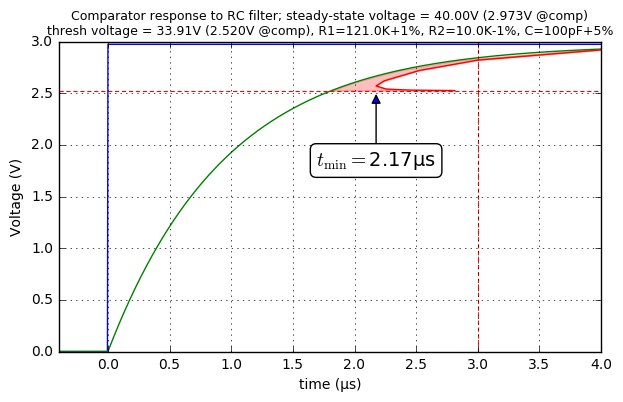
Not bad, that takes about 2.2μs total response. What about 150pF?
show_comparator_response(121e3, 10e3, 150e-12, 0.0145, 0.05)

Um… just past the edge of our 3μs deadline.
I’d probably pick 120pF, which produces a total response time of roughly 2.56μs at the high end of its tolerance, and still has some room to accommodate stray capacitance:
show_comparator_response(121e3, 10e3, 120e-12, 0.0145, 0.05)

Your cheapest 120pF ±5% NP0 50V 0603 capacitor at 1000-piece quantity at Digi-Key is the Waisin 0603N121J500CT at about 1.1 cents each. If you’re willing to use 0402 capacitors, pick the Waisin 0402N121J500CT, at just under 0.77 cents each. (0201 are even cheaper at about 0.66 cents each for the Murata GRM0335C1H121JA01D. If we can live with 100pF, since it’s a more standard value, we can find 0402 Yageo CC0402JRNPO9BN101 capacitors at 0.55 cents each.)
C0G/NP0 capacitors are more stable over temperature than X5R/X7R/Y5V capacitors; they cost more at higher capacitance, but if you’re under 1000pF, generally there’s no significant cost premium to using C0G/NP0 capacitors. This is the kind of capacitor you should use for tight-tolerance filtering; pick the ±5% kind if you can. And at 120pF there’s no cost premium for using 5% tolerance. Finally, the voltage rating of 50 or 100V is “free” if you are at these low capacitance values, so don’t bother trying to optimize and buy a 10V or 25V part to lower cost.
The flip side of filtering: ignoring momentary spikes
We also have a requirement to prevent 100ns pulses from \( V_{OV} - 1.0V \) to 40V reaching \( V_{OV} \) and causing an overvoltage. Let’s check to make sure our 120pF filter capacitor does the trick — actually, to be certain, we’ll use the low side of the capacitor tolerance, 120pF − 5% = 114pF:
t = np.arange(-0.25,3,0.001)*1e-6
dt = t[1]-t[0]
u1 = (t >= 0)*1.0
tpulse = 100e-9
u2 = (t >= tpulse) * 1.0

R1 = 121e3
R2 = 10e3
Rth = 1.0/(1.0/R1 + 1.0/R2)
RC = 120e-12 * 0.95 * Rth

fig = plt.figure(figsize=(7,7))
for row in [1,2]:
    ax = fig.add_subplot(2,1,row)

    for V_OV, label in [(31.572,'minimum $V_{OV}$'),
                        (32.783,'nominal $V_{OV}$'),
                        (33.905,'maximum $V_{OV}$')]:
        v_pre_spike = (V_OV - 1.0)
        v_in = v_pre_spike + (40-v_pre_spike)*(u1-u2)
        dV1 = (40-v_pre_spike)*u1*(1-np.exp(-tpulse/RC))
        y = (v_pre_spike
           + (40-v_pre_spike)*(u1-u2)*(1-np.exp(-t/RC))
           + dV1*u2*(np.exp(-(t-tpulse)/RC))
             )
        y2 = (v_pre_spike
           + (40-v_pre_spike)*u1*(1-np.exp(-t/RC)))
        hl = ax.plot(t,y-V_OV,label=label)
        c = hl[0].get_color()
        ax.plot(t,y2-V_OV, dashes=[4,2],color=c)
        ax.plot(t,v_in - V_OV, linewidth=0.5, color=c)

    ax.plot(t,t*0,'--',color='black')
    if row == 1:
        ax.set_ylim(-1.5,9.5)
    else:
        ax.set_ylim(-1.2,0.5)
    ax.grid(True)
    ax.set_xlim(t.min(), t.max())
    ax.legend(loc='lower right', fontsize=11, labelspacing=0)
    ax.xaxis.set_major_formatter(scale_formatter(1e6))
    ax.set_ylabel(u'$V_{in} - V_{OV}$ (V)', fontsize=13)
    if row == 2:
        ax.set_xlabel(u'time (microseconds)')
fig.suptitle(u'Short pulse rejection: RC=%.2f$\mu$s' % (RC/1e-6),y=0.93);
It does, with some but not a huge amount of margin. (Originally I thought up a pulse requirement of 500ns from \( V_{OV}-0.5V \) to 40V but that did NOT WORK.)
There’s a fine line here: we need a filter that is slow enough that it will block these spikes, but fast enough that it will let overvoltages trip the comparator in less than 3μs.
Other thoughts
Worst-case vs. root-sum-squares
I do most of my work assuming worst-case everywhere. This is like Murphy’s Law on steroids: R1 is at its tolerance limit on the low side, and R2 is at its tolerance limit on the high side, and U2’s reference is on the edge of its tolerance limit, with the right direction for all these factors to conspire against me and give me a worst-case output.
On the whole, this is really unlikely, so much more unlikely than any of the individual components being on the edge of their limit… that it may be overly pessimistic.
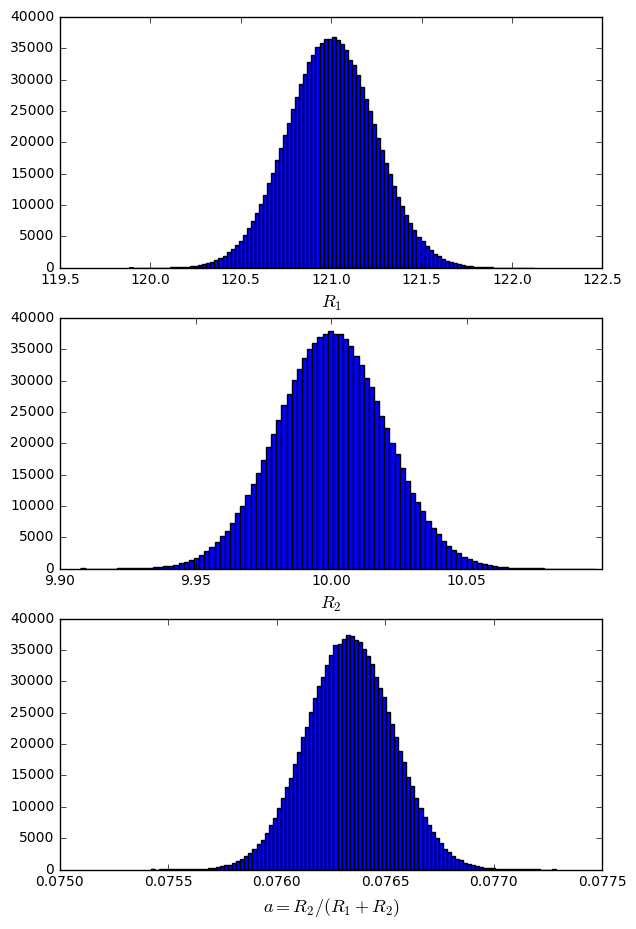
Another approach is to use the root-sum-squares of the individual component tolerances. This is a little naive, because not all of the tolerances weight equally in determining the limits of system variability. But you can use Monte Carlo analysis, where you simulate a large random number of values. For example, let’s just take the voltage divider, and assume those 1% resistors have a Gaussian distribution with a standard deviation of, say, 0.2%. Then we can try a million samples:
np.random.seed(123)

Rstd = 0.002
N = 1000000
R1 = 121e3 * (1 + Rstd*np.random.randn(N))
R2 = 10e3 * (1 + Rstd*np.random.randn(N))
fig = plt.figure(figsize=(7,11))
ax = fig.add_subplot(3,1,1)
ax.hist(R1/1000, bins=100)
ax.set_xlabel('$R_1$',fontsize=13)
ax = fig.add_subplot(3,1,2)
ax.hist(R2/1000, bins=100)
ax.set_xlabel('$R_2$',fontsize=13)
a = R2/(R1+R2)
ax = fig.add_subplot(3,1,3)
ax.hist(a, bins=100)
ax.set_xlabel('$a=R_2/(R_1+R_2)$',fontsize=13)
import pandas as pd

def get_stats(x):
    x0 = np.mean(x)
    s = np.std(x)
    dev = max(np.max(x-x0), np.max(x0-x))
    return dict(mean=x0, max=np.max(x), min=np.min(x),std=s,
               normstd=s/x0, normdev=dev/x0)

df = pd.DataFrame([get_stats(x) for x in [R1, R2, a]], index=['R1','R2','a'],
                 columns=['mean','min','max','std','normstd','normdev']).transpose()
def tagfunc(x):
    return pd.Series([('K'
                       if x.name.startswith('R') and not k.startswith('norm')
                       else 'ratio',
                       x[k])
                       for k in x.index], x.index)
def formatfunc(x):
    tag, v = x
    if tag == 'K':
        return '%.3f K' % (v*1e-3)
    else:
        return '%.5f' % v

df.apply(tagfunc).style.applymap(lambda cell: 'text-align: right').format(formatfunc)| R1 | R2 | a | |
|---|---|---|---|
| mean | 121.000 K | 10.000 K | 0.07634 |
| min | 119.885 K | 9.908 K | 0.07542 |
| max | 122.120 K | 10.097 K | 0.07729 |
| std | 0.242 K | 0.020 K | 0.00020 |
| normstd | 0.00200 | 0.00200 | 0.00261 |
| normdev | 0.00925 | 0.00973 | 0.01245 |
The table above is somewhat terse:
- a is the voltage divider ratio
- mean is the mean value \( \mu_x \) of all samples
- min is the minimum value \( x_\min \) of all samples
- max is the maximum value \( x_\max \) of all samples
- std is the standard deviation \( \sigma_x \) of all samples
- normstd is the normalized standard deviation (\( \sigma_x/\mu_x \))
- normdev is the normalized worst-case deviation = \( \max(x_\max-\mu_x, \mu_x-x_\min)/\mu_x \)
For this set of samples, the worst-case deviation of R1 is 0.925%, the worst-case deviation of R2 is 0.973%, and the worst-case deviation of a is 1.245%.
Compare these results with a worst-case analysis approach if someone told us R1 had 0.925% tolerance and R2 had 0.973% tolerance:
R1_nom = 121e3
R2_nom = 10e3
a_nom = R2_nom/(R1_nom+R2_nom)
def showsign(x):
    return '-' if x < 0 else '+'
for s in [-1,+1]:
    R1 = R1_nom*(1+s*0.00925)
    R2 = R2_nom*(1-s*0.00973)
    a = R2/(R1+R2)
    print "R1=121K%s0.925%%, R2=10K%s0.973%% => a=%.5f = a_nom*%.5f (%+.2f%%)" % (
        showsign(s), showsign(-s), a, a/a_nom, (a/a_nom-1)*100
    )
R1=121K-0.925%, R2=10K+0.973% => a=0.07768 = a_nom*1.01767 (+1.77%) R1=121K+0.925%, R2=10K-0.973% => a=0.07501 = a_nom*0.98260 (-1.74%)
In other words, Monte Carlo analysis gives us a bound of ±1.245% for the voltage divider ratio, but worst-case analysis gives us a bound of ±1.77% for the voltage divider ratio.
Worst-case analysis is always pessimistic (assuming you’ve taken into account all possible factors that produce error — which is not easy, or even practical… but the major ones are going to be component tolerance and temperature coefficients, and that’s about the best you can do) and Monte Carlo analysis is… optimistic? realistic? The problem is that you can’t tell unless you know the error distributions.
If I buy a reel of ±1% surface-mount chip resistors, I have absolutely no idea what the distribution of their resistance is going to be, except they’ll all be very likely to be within 1% of their nominal values at 25°C, because that is what the manufacturer claims. Suppose I’ve got a reel of 5000 10kΩ resistors. Then 2500 of them could measure 10.1kΩ and 2500 could measure 9.9kΩ. Or they might all be 10.1kΩ. Or they might be uniformly distributed between 9.9kΩ and 10.1kΩ. Or they might have a tight normal distribution around 9.93kΩ (say, a mean of 9.93kΩ and standard deviation 2.4Ω) for this reel, but if I buy another reel manufactured from a different batch of raw materials, then they might have a similar tight normal distribution around 10.02kΩ. Maybe the resistors manufactured on Thursday nights are typically 20 ohms greater than other manufacturers, because the factory foreman is a stupid jerk and likes the temperature in his factory to be a few degrees warmer than the 20°C ± 1°C specified by the company’s engineering staff, and that throws off some of the manufacturing processes slightly.... most likely that would still pass the 1% tolerance test, although the foreman should be fired for adding unnecessary sources of error.
The distributions are likely to be somewhat Gaussian. It’s just that you can’t trust that to be the case. There’s an apocryphal story I read somewhere, but cannot find, and is probably false, that long ago, the 1% resistors and 5% resistors were two different grades from the same manufacturing process, in other words:
- each resistor was measured
- if the resistor was within 1% of nominal, it went into the 1% pile
- if the resistor was not within 1% of nominal, but was within 5% of nominal, it went into the 5% pile
- if the resistor was not within 5% of nominal, it went into the trash
This kind of case could produce some strange distributions:
np.random.seed(123)

Rnom = 10e3
R = Rnom * (1 + 0.015*np.random.randn(N))

bin_size = 0.002
bins = np.arange(0.92,1.08001,bin_size) * Rnom
counts, _ = np.histogram(R,bins=bins)
bin_center = (bins[:-1] + bins[1:])/2.0

selections = [('1%', 'green',lambda x: abs(x-1) <= 0.01),
              ('5%', 'yellow',lambda x: ((0.01 < abs(x-1)) & (abs(x-1) <= 0.05))),
              ('reject', 'red',lambda x: 0.05 < abs(x-1))]

fig=plt.figure(figsize=(7,4))
ax=fig.add_subplot(1,1,1)
for name, color, select_func in selections:
    ii = select_func(bin_center/Rnom)
    ax.bar(bin_center[ii], counts[ii], width=bin_size*Rnom,
           color=color, label='%s (N=%d)' % (name, sum(counts[ii])))
ax.set_xlim(0.92*Rnom, 1.08*Rnom)
ax.legend(fontsize=12, labelspacing=0)
ax.set_title('Distribution of resistors selected from $\\sigma=0.015$')
ax.set_xlabel('resistance (ohms)')
ax.set_ylabel('count')
<matplotlib.text.Text at 0x10e44d610>
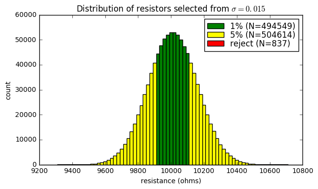
Here we have a normal distribution with \( \sigma=0.015 R \) (150 ohms).
- about half of them are 1% resistors with the green distribution: mostly uniformly distributed with a slight clustering around nominal
- about half are 5% resistors with the yellow distribution: a normal distribution with a gap in the center; most are in the 1-2% tolerance range
- around 0.08% of them are rejected because they’re more than 5% from nominal
Numerical answers for this Gaussian distribution — rather than samples from a Monte Carlo process — can be determined using the cumulative distribution function scipy.stats.norm.cdf:
import scipy.stats

stdev = 0.015
def cdf_between(r1, r2=None):
    cdf1 = scipy.stats.norm.cdf(r1/stdev)
    if r2 is None:
        return 1-cdf1
    else:
        return scipy.stats.norm.cdf(r2/stdev)-cdf1

# the 2* is to capture left-side and right-side distributions
N1pct = 2*cdf_between(0,0.01)
N5pct = 2*cdf_between(0.01,0.05)

ranges = [0, 0.005, 0.01, 0.02, 0.05]
for i, r0 in enumerate(ranges):
    cdf0 = scipy.stats.norm.cdf(r0/stdev)
    try:
        r1 = ranges[i+1]
        tail = False
    except:
        r1 = None
        tail = True
    fraction = 2*cdf_between(r0,r1)
    if not tail:
        print "%.1f%% - %.1f%%: %.6f (%.2f%% of %d%% tolerance)" % (r0*100,r1*100,fraction,
                                                         fraction/(N1pct if r0 < 0.01 else N5pct)*100,
                                                         1 if r0 < 0.01 else 5)
    else:
        print "     > %.1f%%: %.6f" % (r0*100,fraction)

print "%.6f: 1%% tolerance" % N1pct
print "%.6f: 5%% tolerance" % N5pct
0.0% - 0.5%: 0.261117 (52.75% of 1% tolerance)
0.5% - 1.0%: 0.233898 (47.25% of 1% tolerance)
1.0% - 2.0%: 0.322563 (63.98% of 5% tolerance)
2.0% - 5.0%: 0.181564 (36.02% of 5% tolerance)
> 5.0%: 0.000858
0.495015: 1% tolerance
0.504127: 5% tolerance
- 49.50% of these apocryphal resistors were graded as 1%
- 52.75% of them less than 0.5% from nominal
- 47.25% of them between 0.5% and 1% tolerance
- 50.41% of these apocryphal resistors were graded as 5%
- 63.98% of them between 1% and 2% tolerance
- 36.02% of them between 2% and 5% tolerance
- 0.09% of these apocryphal resistors were more than 5% from nominal
Grading may still be done for some electronic components (perhaps voltage references or op-amps), but it’s not a great manufacturing strategy. The demand for different grades may fluctuate with time, and is unlikely to match up perfectly with the yields from various grades. Suppose that you are the manufacturing VP of Danalog Vices, Inc., which produces the DV123 op-amp in two grades:
- an “A” grade op-amp with input offset voltage less than 1mV
- a “B” grade op-amp with 1mV - 5mV input offset.
Suppose also that the manufacturing process ends up with 40.7% in the “A” grade, 57.2% in the “B” grade, and 2.1% as yield failures.
Maybe in 2019, there were orders for 650,000 DV123A op-amps and 800,000 DV123B op-amps. To meet this demand, Danalog Vices fabricated wafers with enough dice for 1.8 million parts: 732,600 DV123A, 1,029,600 DV123B, and 37,800 yield failures, meeting demand and a little extra. At the end of the year, there are 82,600 excess DV123A in inventory and 229,600 excess DV123B in inventory.
Now in 2020, the forecasted orders are 900,000 DV123A and 720,000 DV123B op-amps. (Some major customer decided they needed higher precision.) You don’t have many options here… making 2.2 million dice would produce 895,400 DV123A op-amps and 1,258,400 DV123B op-amps. Combined with the previous year’s inventory, this would be enough to meet demand plus 78,000 extra DV123A op-amps and 768,000 DV123B. Tons of excess B grade op-amps.
That’s not going to work very well. If the fraction of customer orders of A grade parts is much higher than the natural yield of A grade parts, then there will be an excess of B grade parts. If we had too many A grade op-amps, Danalog Vices could package and sell them as B grade op-amps, but an excess of B grade op-amps will end up as scrapped inventory.
There’s no realistic way to shift the manufacturing process to make more A grade op-amps through grading alone. We could add a laser-trimming step on the manufacturing line to improve B-grade dice until they meet A-grade specs, which adds some cost.
To jump out of this grading quagmire and back to the overall point I am trying to make: you cannot be sure of the error distribution of components. Can’t can’t can’t. The best you might be able to do is get characterization data from the manufacturer, but this would be for one sample batch and may not be representative of the manufacturing process through the product’s full life cycle.
Characterization data
Whether you will find this characterization data in the datasheet is really hit-or-miss. Some datasheets don’t have it at all. Some have limited information, as in the LM2903B datasheet:

The datasheet lists a specification as ±2.5mV offset voltage at 25°C. The characterization graph shows 62 samples within ±1.0mV offset voltage, with little variation over temperature.
A more detailed example of this type of characterization data is from the MCP6001 op-amp datasheet, which shows histograms of input offset voltage, offset voltage tempco, the offset voltage curvature or quadratic temperature coefficient (!), and input bias current.
Here’s Figure 2-1, showing an offset voltage histogram of around 65000 samples:

The MCP6001 datasheet claims ±4.5mV maximum at 25°C. I crunched some numbers based on reading the histogram and came up with a mean of −0.3mV with a standard deviation of σ=1.04mV; if this were representative of the population as a whole, then the limits of ±4.5mV are roughly −4σ and +4.6σ, and for a normal distribution, would have expected yield failures of roughly 32ppm below −4.5mV and 2ppm above 4.5mV. (These are just the results of scipy.stats.norm.cdf(-4) and scipy.stats.norm.cdf(-4.6).)
The main value of the characterization graphs (to me, at least) are not as numerical data that I can depend on directly, but rather that they show a roughly Gaussian distribution (and not, say, a uniform distribution) and show how conservative the manufacturer is in choosing minimum/maximum limits given this characterization data. You hear “six sigma” bandied about a lot — which can be interpreted in one way as having limits equal to six standard deviations from the mean — and for a Gaussian distribution, this represents about 2 failures per billion samples covering both low-end and high-end tails. (2*scipy.stats.norm.cdf(-6))
Note, however, the fine print at the beginning of the Typical Performance Curves section of the MCP6001 datasheet:
The graphs and tables provided following this note are a statistical summary based on a limited number of samples and are provided for informational purposes only. The performance characteristics listed herein are not tested or guaranteed. In some graphs or tables, the data presented may be outside the specified operating range (e.g., outside specified power supply range) and therefore outside the warranted range.
So use the specifications! I recommend you ignore worst-case analysis only at your own peril.
Mitigating strategies
We’ve talked a lot about how different sources of error — resistance tolerance, comparator input offset voltage, temperature coefficients, etc. — contribute to total uncertainty of a circuit parameter like threshold voltage. It paints a grim picture; you will find that except for the simplest of circuits, it is hard to provide an overall error of less than 1%.
There are, however, ways to compensate for the effects of component tolerances. I count at least three:
- we can use ratiometric design techniques to reduce the effect of certain error sources
- we can calibrate our circuitry
- we can use digital signal processing to reduce the need for components with tolerance
Ratiometric design
Ratiometric design is a method of circuit design where measurements are made of the ratio of two quantities rather than their absolute values. If they share some common source of error, then that error will cancel out. I talked about this in an article on thermistor signal conditioning. If I have a 3.3V supply feeding a voltage divider, and the same 3.3V supply used for an analog-to-digital converter, then the ADC reading will be the voltage divider ratio \( R2/(R1+R2) \) — plus ADC gain/offset/linearity errors — and will not be subject to any variation in the 3.3V supply itself.
Or, suppose there are reasons to avoid a voltage divider configuration, and instead I need a current source to drive a resistive sensor, as shown in the left circuit below:

Here the ADC reading (as a fraction of fullscale voltage \( V_{ref} \)) is \( I_0R_{sense}/V_{ref} \), which is sensitive to errors in both the current \( I_0 \) and the voltage reference \( V_{ref} \).
We can handle this resistive sensor ratiometrically with the circuit on the right, by using a reference resistor \( R_{ref} \) and a pair of analog multiplexers U1, U2. Here we have to take two readings, \( x_1 = I_0R_{sense}/V_{ref} \) and \( x_2 = I_0R_{ref}/V_{ref} \); if we divide them, we get \( x_1/x_2 = R_{sense}/R_{ref} \) which is sensitive only to tolerances in the two resistors; variations in current \( I_0 \) and voltage \( V_{ref} \) cancel out.
Calibration
Calibration involves a measurement of an accurate, known reference. If I have some device with some measurement error that is consistent — for example a gain and offset — then I can measure one or more known inputs during a calibration step, and use those measurements to compensate for device errors.
One very common instance of calibration is the use of a tare weight with a scale — the weight of a platform or container is unimportant, so when that platform or container is empty, we can weigh it and use the measurement as a reference to subtract from a second measurement. When you go to the deli counter at a supermarket and get a half-pound or 200g of sliced turkey, the scale is automatically calibrated to an empty measurement first; then the weight of the turkey is determined using a measurement relative to the empty measurement.
That kind of measurement calibrates out the offset but not the gain; a gain calibration would require some standard weight to be used, like a standard 1kg weight.
Calibration can be done during manufacturing with external equipment (1kg weights, voltage or temperature standards, etc.) — this can be somewhat time-consuming or costly. After manufacturing, such measurements are possible only at limited times and with substantial expense.
The most important aspect of relying on calibration is to ensure that the calibration measurements remain valid.
If a circuit is prone to voltage offset, and we want to use calibration to compensate for that offset, we need to ensure that the offset does not change significantly during the time of use: drift due to time and temperature changes can eliminate the benefit of calibration. In fact, excessive drift can make a measurement using calibration worse than without that calibration — suppose some device measures voltage and has a worst-case accuracy of 2mV. The voltage offset during calibration might be +1.4mV; if it drifts to −1.4mV then the resulting accuracy including calibration is 2.8mV error. So measurement drift is a serious concern. Tare weight is an easy circumstance to avoid the effects of drift: people or sliced turkey or trucks on a scale can be measured a few seconds after a tare step to calibrate out offset, which is generally too short for changes in temperature or time drift. On the other hand, laboratory test equipment like oscilloscopes or multimeters typically are used for 12 months between calibrations, so they need to be designed for low drift and low temperature coefficient.
Digital signal processing
DSP can also help to remove the need for analog components that introduce errors. Analog signal conditioning is still necessary to handle low-level amplification and high-frequency issues, but other operations like squaring or logarithms or filtering or applying temperature compensation can be done in the digital domain, where numeric errors can be made arbitrarily small.
One of the major achievements of DSP has been in equalization in communications. 56K dialup modems and DSL both represent a triumph of DSP over the limitations of analog signal processing. We now take it for granted that we have Internet bandwidths of 40Mbps. I remember the old acoustic-coupled 300-baud modems: imagine transmitting a file at 30 bytes per second. That’s about 2.6 megabytes per day. There’s only so much you can do with analog signal conditioning before you run into the challenges of component tolerances. DSP eliminates all that — assuming you can sample and process the data fast enough.
Just make sure to avoid using software as an overused crutch — the mantra of “Oh, we can fix that in software” makes me cringe. If there are design errors in the analog domain, they can be much more complex and costly to fix (and verify!) in the digital domain. Mismatches in components or noise coupling are problems that should be handled before they get inside a microcontroller. One of my pet peeves is the use of single-ended current-sense amplifiers in motor drives. Current sense resistors are relatively inexpensive these days: you can buy 10mΩ 1% 1W 1206 chip resistors for less than 10 cents in quantity 1000 that will produce a high-quality current sense signal without adding a lot of extra voltage drop. But they should be used with a differential amplifier to remove the effects of common-mode voltage that results from parasitic circuit resistance and inductance. This common-mode voltage is hard (if not impossible) to “just fix in software” — it can change with temperature, causes undesirable errors in analog overcurrent sensing, and can introduce coupling between current paths in the circuit.
Sources of measurement error need to be well-understood. The overvoltage circuit I discussed in this article is a good example; if I just design a circuit and build it and consider it done because “well, it seems to work”, then every source of error represents a latent risk in my design. Understanding and bounding those risks is the key to a successful design.
Wrapup
Today we went through a grand tour around the idea of component tolerances.
We looked at this overvoltage detection circuit:
- R1 = 121kΩ
- R2 = 10.0kΩ
- R3 = 2.00kΩ
- R4 = 1.00kΩ
- R5 = 1.00MΩ
- R6 = 5.1kΩ
- U1 = 1/2 LM2903B
- U2 = NCP431B
- C1 = 56pF
- C2 = 100pF
We examined the various sources of component tolerance error, including:
- static errors
- mismatch of R1 / R2
- other sources of error besides the “1%” tolerance listed on a bill of materials (for example, temperature coefficient and mechanical strain)
- accuracy of voltage reference U2
- comparator input offset voltage and input bias current
- dynamic errors
- noise filtering with C1
- comparator response time vs. overdrive
We talked about some aspects of selecting the voltage reference and comparator, and about comparator hysteresis.
We explored the use of statistical analysis (Monte Carlo methods) as a more optimistic alternative to worst-case analysis, and investigated the issues of component error distribution.
Finally, we looked at methods of mitigating component error:
- ratiometric measurements
- calibration
- digital signal processing
Along the way, we touched upon a number of minor tangents:
- the price of 5% / 1% / 0.5% / 0.1% chip resistors
- irreversible resistance changes upon soldering into a PCB
- voltage divider error sensitivity to resistor tolerance, as a function of the nominal voltage divider ratio \( \alpha \), namely \( S \approx 2(1-\alpha). \) So a voltage divider ratio near 1 has hardly any error, whereas small voltage divider ratios almost double the resistor tolerance: a 10:1 voltage divider using 1% resistors can have a worst-case error of approximately 2%.
- the internal architecture of the LM393 comparator
- grading of components based on measured values
I hope you take away some useful techniques for managing component error in your next project.
Thanks for reading!
© 2020 Jason M. Sachs, all rights reserved.


- Comments
- Write a Comment Select to add a comment
To post reply to a comment, click on the 'reply' button attached to each comment. To post a new comment (not a reply to a comment) check out the 'Write a Comment' tab at the top of the comments.
Please login (on the right) if you already have an account on this platform.
Otherwise, please use this form to register (free) an join one of the largest online community for Electrical/Embedded/DSP/FPGA/ML engineers:


