


Digital PLL’s, Part 3 – Phase Lock an NCO to an External Clock
Sometimes you may need to phase-lock a numerically controlled oscillator (NCO) to an external clock that is not related to the system clocks of your ASIC or FPGA. This situation is shown in Figure 1. Assuming your system has an analog-to-digital converter (ADC) available, you can sync to the external clock using the scheme shown in Figure 2. This time-domain PLL model is similar to the one presented in Part 1 of this series on digital PLL’s [1]. In that PLL, we dealt with phases only, which resulted in a very simple model. Here, we have a sinusoidal reference signal instead of a phase reference signal, so we need to make some modifications.
Our new model adds a Hilbert transformer and a complex digital phase detector (PD). The Hilbert transformer converts the real input to a complex signal. The complex PD compares the phase of this signal to that of the complex sinusoidal output of the NCO. The model includes ADC quantization noise and the Gaussian noise of the ADC and external clock, allowing us to examine how they affect the NCO output phase noise. However, the model does not include the phase noise contributions of the PLL sample clock or the external clock.
In this post, I’ll describe the components of the PLL and then perform a couple of simulations. A word of caution: I have not implemented this design in hardware, so there may be gotchas with the approach that I have not anticipated.
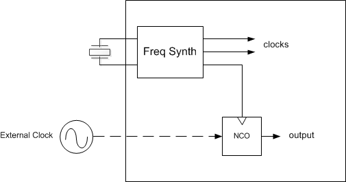
Figure 1. How do you phase-lock the NCO to an external clock that is unrelated to the system clocks?
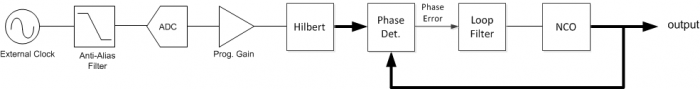
Figure 2. PLL to phase-lock an NCO to an external clock (wide lines are complex signals).
Hilbert Transformer
Here we’ll use the same 31-tap Hilbert transformer presented in an earlier post [2]. Its Matlab code is part of the m-file listed in the Appendix. For sinusoidal input, the Hilbert Transformer generates I and Q sinusoids, with Q lagging I by π/2. The pure-imaginary frequency response of Q/I is plotted in Figure 3. For sample frequency of 40 MHz, this design allows an input frequency range of roughly 4 MHz to 16 MHz (flat region of the response).
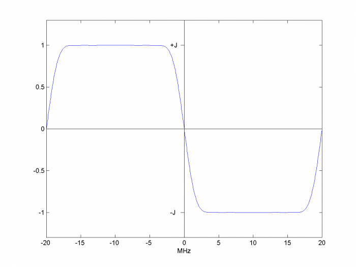
Figure 3. Frequency Response of Hilbert Transformer, fs = 40 MHz.
Complex Digital Phase Detector
In the following, we refer to the external clock as the reference clock, and we make the simplifying assumption that it is sinusoidal. The phase detector computes the phase difference of two complex sinusoidal inputs [3]. A conceptual block diagram of this remarkably simple device is shown in Figure 4. Note that the NCO input has a negative exponent (inverted phase). The output is simply the imaginary part of the complex product of the two inputs:
$$y=Im\{A\ exp(j(\omega t+\phi_{ref}))\cdot exp(-j(\omega t+\phi_{nco}))\} = Im\{A\ exp(j(\phi_{ref}-\phi_{nco})\}$$
$$y= A\ sin(\phi_{ref} - \phi_{nco}) \qquad $$
$$y= -A\ sin(\phi_{nco} - \phi_{ref}) \qquad (1)$$
The terms involving ω have canceled, leaving a slowly rotating or stationary phase difference. Equation 1 is plotted in Figure 5 for A = 1. The useful phase error range is from -1/4 to +1/4 cycles or –π/2 to +π/2 radians. The phase detector gain is the slope of the curve near zero, which (since sin(x) ~= x for small x) is -A rad-1. The gain in cycles-1 is thus -2πA.
Given phase detector inputs Iref/Qref and Inco/-Qnco (where the negative sign inverts the NCO phase), the output is:
$$y= Im\{(I_{ref}+jQ_{ref})(I_{nco}-jQ_{nco})\}$$
$$y= -I_{ref}Q_{nco} + Q_{ref}I_{nco}\qquad (2)$$
Equation 2 is implemented by the block diagram in Figure 6. As you can see, just two multipliers and an adder are used.
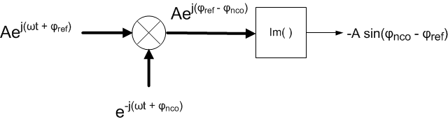
Figure 4. Complex Digital Phase Detector Conceptual Diagram (wide lines are complex).
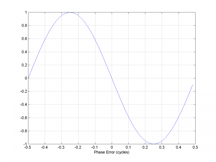
Figure 5. Phase Detector Characteristic, sinusoidal input amplitude = 1.
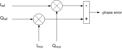
Figure 6. Implementation of Complex Digital Phase Detector.
Loop Filter
I discussed calculation of the loop filter coefficients for a 2nd order PLL in Part 2 [4]. The formulas for the coefficients are:
$$ K_L= \frac{2\zeta \omega_n}{K_p} \cdot \frac{T_s}{K_{nco}}\qquad(3)$$
$$ K_I= \frac{\omega_n^2}{K_p} \cdot \frac{T_s^2}{K_{nco}}\qquad(4)$$
Where KL and KI are the proportional and integrator gains of the loop filter in Figure 7, and the other parameters are defined as follows:
ζ desired loop damping factor (dimensionless)
ωn desired loop natural frequency, rad/s
Kp phase detector gain, cycle-1
Knco nco gain (dimensionless)
Ts sample time, s
In the model, I have assumed the reference clock is a sine with amplitude A = 1. This gives phase detector gain Kp = 2π cycles-1. I used damping factor ζ = 1.
For larger values of loop natural frequency, KL may be greater than one, causing the loop filter output level to exceed +/- 1 during acquisition. The loop filter output should clip (not roll-over). Clipping can hurt acquisition, so typically the clip level is set higher than the expected excursion of the loop filter output. It may be appropriate to set clip level to a value greater than +/-1.
NCO
We developed the difference equations for the NCO (shown in Figure 7) in Part 1 [1]. The NCO used here has a couple of modifications from the Part 1 example:
- We quantize the phase to 20 bits and the I/Q outputs to 12 bits.
- In Part 1, we used the NCO’s phase output as the input to the phase detector; here we use the NCO’s sine and cosine outputs.
The model uses the Matlab sin and cos functions and thus does not provide a method of computing those outputs. For a description of a look-up table (LUT) approach for computing sine and cosine, see [5]. For a description of a Cordic approach, see [6].
Anti-alias Filter, ADC, and Programmable Gain
An anti-alias filter is needed to filter clock harmonics and noise at frequencies above fs/2. The ADC input does not have to be a pure sinusoid; for example, if the third harmonic of the clock is below fs/2, the anti-alias filter does not need to attenuate it.
The model assumes an 8-bit ADC using the same sample rate as the NCO, and includes Gaussian noise on the input clock. This noise represents noise of the clock source and the input noise of the ADC. The SNR due to quantization noise of an ideal 8-bit ADC is 6.02*8 + 1.76 dB = 49.9 dB [7]. I somewhat arbitrarily chose a Gaussian noise amplitude σ = 0.0015 (See Appendix for Matlab code: .0015*randn(1,N) ). For input clock amplitude = 1 V peak = .707 V rms, this gives an SNR of 20 log10(.707/.0015) = 53.5 dB. Thus the Gaussian noise is 3.6 dB below the quantization noise.
The gain of the phase detector is proportional to the reference clock level. The model does not include it, but a programmable gain block (or AGC), as shown in Figure 7, would be useful for setting the reference clock level. The gain might have programmable values of 1, 9/8, 10/8, … etc. For example, given an ADC full-scale input of 2 Vpp, if the clock level at the ADC input were 1.5 Vpp, the programmable gain could be set to 10/8, giving a clock level at the Hilbert transformer input of 1.5/2 * 10/8 = 0.94 with respect to full-scale.
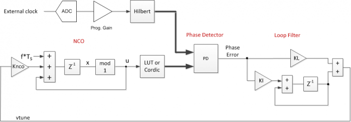
Figure 7. PLL Block Diagram showing NCO and Loop Filter parameters.
Simulation Example 1
This time-domain simulation solves the difference equations of the 2nd-order PLL, as was done in Part 1. The PLL model in Part 1 did not include quantization. Here, I have quantized a few key signals: the ADC output; the NCO phase and NCO output; also the Hilbert transformer coefficients. The m-file for this simulation is provided in the Appendix. Table 1 lists the parameter values used.
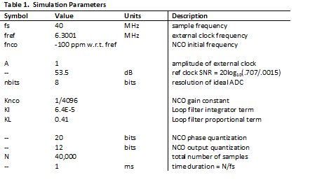
Note that the values of KI and KL used result in loop natural frequency of 2 KHz, with damping of 1.0. For a real-world design, we’d probably want to use a lower natural frequency (to minimize spurs and noise from the ADC), but I chose this value to keep simulation time manageable. Note that the loop bandwidth of the PLL is slightly greater than the natural frequency. The external clock frequency is 6.3001 MHz, and the NCO initial frequency is 100 ppm (630.01 Hz) below that.
The simulation results are shown in Figures 8 through 12. Figure 8 shows the spectrum of the reference clock at the output of the 8-bit ADC. The highest spur is roughly 75 dB below the carrier level. Figure 9 shows the output of the phase detector as the loop acquires lock. The fuzz on this signal is caused by the Gaussian noise and ADC quantization noise. Figure 10 shows the loop filter output (vtune). Figure 11 shows the spectrum of the NCO cosine output signal. The close-in spectrum of the NCO output is shown in Figure 12. Note that the model does not include the phase noise of the PLL sample clock.
In Figure 11, the highest spur is more than 100 dB below the carrier level – an improvement of more than 25 dB compared to the spurious at the ADC output. This occurs because the spurious level outside the 2 kHz bandwidth of the PLL is attenuated by the PLL’s closed-loop response [4]. But given that the noise is amplitude noise, how does it affect the PLL at all? In the phase domain, you can view the noise as a vector modulating the tip of the clock signal [8] (See Figure 14 in the next example). The vector has an amplitude and phase component. The amplitude component does not affect the PLL. The phase component, if inside the loop bandwidth, appears as noise in the NCO output. If outside the loop bandwidth, it is attenuated by the closed-loop response of the PLL.
Keep in mind that in a particular hardware implementation, spurs may fall within the loop bandwidth and thus will not be attenuated by the PLL. The next example looks more closely at the attenuation of noise outside the PLL loop bandwidth.
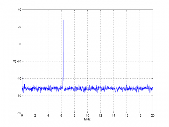
Figure 8. Spectrum at ADC output.
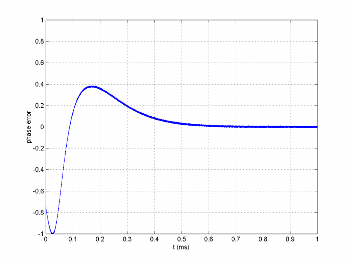
Figure 9. Phase Detector Output.
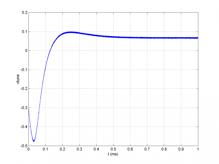
Figure 10. Loop Filter Output (vtune).
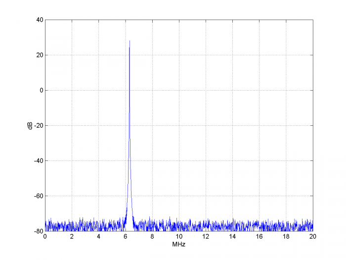
Figure 11. Spectrum of NCO cosine output.
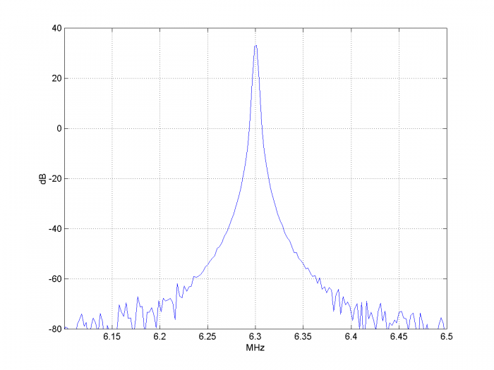
Figure 12. Close-in spectrum of NCO cosine output. Span = 400 kHz.
Simulation Example 2
In this example, we’ll look at how the PLL’s closed-loop response shapes the noise of the reference signal. We’ll use most of the same parameters as in Example 1, but we’ll increase the Gaussian noise level. We’ll also change the loop natural frequency to 20 kHz and reduce the number of samples. These new parameters are coded as follows:
    N= 20000                               % number of samples
    Vr= A*cos(phi_r) + .05*randn(1,N);     % ref clock with Gaussian noise
    KI= .0064;                          % loop filter integrator gain, fn = 20 kHz
    KL= 4.1;                            % loop filter proportional gain, fn= 20 kHz
The reference clock SNR is 20log10(.707/.05) = 23 dB. It has the spectrum shown in the top of Figure 13. The spectrum of the NCO cosine output is shown in the bottom of Figure 13. You can see the shape of the PLL closed-loop response in the noise floor.
Figure 14 is a polar plot of the I/Q output of the Hilbert transformer, derotated to baseband. As discussed in Example 1, you can see that the phase vector is amplitude and phase modulated by the Gaussian noise (the noise causes the amplitude to exceed 1.0, which is a little flakey for a real application, but it works to demonstrate the concept). The phase detector computes the error due to the phase modulation, and the PLL attenuates components of the phase modulation outside the loop bandwidth. Figure 15 shows the I/Q output of the NCO, derotated to baseband: you can see that the phase noise is much less than that of the reference clock. Again, the model does not include the phase noise of the PLL sample clock. Figure 16 shows the increased NCO phase noise that results when fn is widened to 200 kHz.
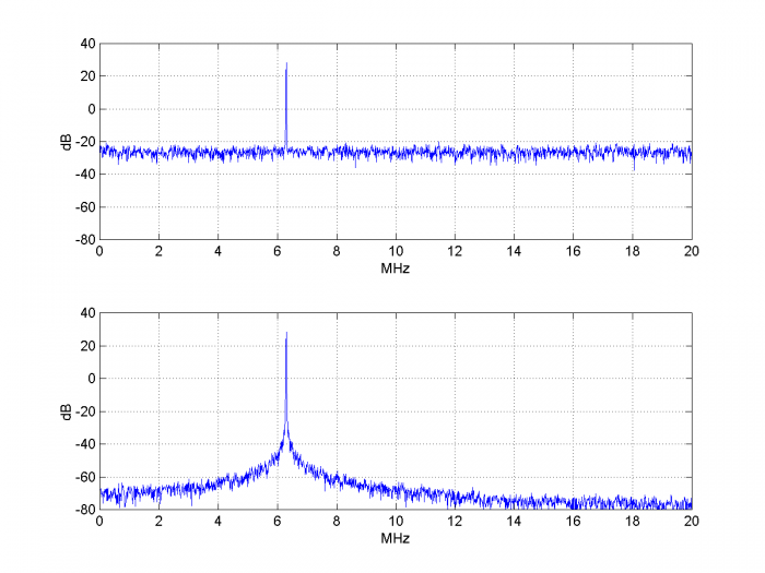
Figure 13. Top: Spectrum of reference clock with added Gaussian noise. psd(Vr,2^12,fs/1e6)
Bottom: Spectrum of NCO output for loop fn = 20 kHz. psd(y(5000:end),2^12,fs/1e6)
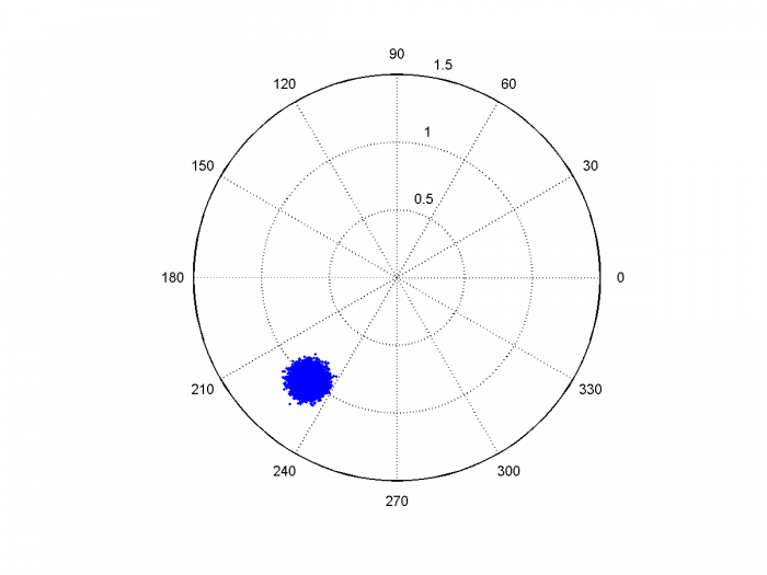
Figure 14. De-rotated phase of Hilbert Transformer output, showing Gaussian noise of reference clock.
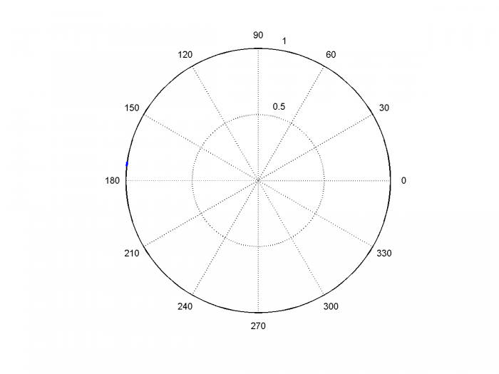
Figure 15. De-rotated phase of NCO output, fn = 20 kHz.
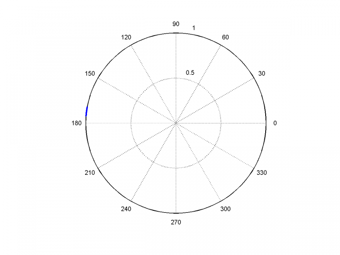
Figure 16. De-rotated phase of NCO output, fn = 200 kHz.
References
1. Robertson, Neil, “Digital PLL’s – Part 1”, June, 2016 https://www.dsprelated.com/showarticle/967.php
2. Robertson, Neil, “Phase or Frequency Shifter Using a Hilbert Transformer”, March, 2018,
https://www.dsprelated.com/showarticle/1147.php
3. Gardner, Floyd M., Phaselock Techniques, 3rd Ed., Wiley-Interscience, 2005, section 13.1.3.
4. Robertson, Neil, “Digital PLL’s – Part 2”, June, 2016
https://www.dsprelated.com/showarticle/973.php
5. Rice, Michael, Digital Communications, a Discrete-Time Approach, Pearson Prentice Hall, 2009, section 9.2.2.
6. Rice, section 9.4.
7. Kester, Walt, Ed., The Data Conversion Handbook, Newnes, 2005 Ch 2.
http://www.analog.com/en/education/education-library/data-conversion-handbook.html
8. Brannon, Brad, “Sampled Systems and the Effects of Clock Phase Noise and Jitter”, Analog Devices Application Note AN-756, 2004
http://www.analog.com/media/en/technical-documentation/application-notes/AN-756.pdf
Neil Robertson May, 2018
Appendix Matlab time-domain model of PLL with external reference clock
% pll_ext_clk1.m5/23/18 Neil Robertson
% Digital PLL model in time using difference equations.
% External reference clock and complex digital phase detector
% fn = 2 kHzNCO initital freq error = -100ppm
%
N= 40000;                            % number of samples
fref= 6.3001e6;                      % Hz  external clock frequency
fs= 40e6;                            % Hz sample rate
Ts = 1/fs;                           % sample time
n= 0:N-1;                            % time index
t= n*Ts*1000;                        % ms
%
% 31-tap Hilbert xfmr
b= 2/pi * [-1/15 0 -1/13 0 -1/11 0 -1/9 0 -1/7 0 -1/5 0 -1/3 0 -1 0 1 0 ...
1/3 0 1/5 0 1/7 0 1/9 0 1/11 0 1/13 0 1/15];
b1= b.*blackman(31)';                % windowed coefficients
b1= round(b1*2^12)/2^12;
b2= [0 0 0 0 0 0 0 0 0 0 0 0 0 0 0 1];          % delay of 15 samples (CT of filter)
%
% Create reference signal
A = 1.0;                                        % reference signal amplitude
Vr= A*cos(2*pi*fref*n*Ts) + .0015*randn(1,N);   % ref signal with Gaussian noise
nbits= 8;
Vr= floor(2^(nbits-1)*Vr)/2^(nbits-1);          % ADC quantization of ref signal
% Apply reference signal to Hilbert transformer
Ir= filter(b2,1,Vr);                            % I channel HT output
Qr= filter(b1,1,Vr);                            % Q channel HT output
%
% PLL
Knco= 1/4096;                                    % NCO gain constant
KI= 6.4e-5;                                % loop filter integrator gain, fn= 2 kHz
KL= 0.41;                                  % loop filter linear gain, fn= 2 kHz
fnco = fref*(1-100e-6);                    % Hz NCO initial frequency
u(1) = 0;
int(1)= 0;
phase_error(1)= 0;
vtune(1) = 0;
% Compute difference equations
for n= 2:N;
    % NCO
    x = fnco*Ts + u(n-1) + vtune(n-1)*Knco;        % cycles NCO phase
    u(n) = mod(x,1);                               % cycles NCO phase mod 1
    u(n)= fix(2^20*u(n))/2^20;                     % quantized phase 20 bits
    Inco = cos(2*pi*u(n-1));
    Qnco = sin(2*pi*u(n-1));
    y(n)= round(2^11*Inco)/2^11;                   % quantized NCO output 12 bits
    % Phase Detector
    pe= -Ir(n-1)*Qnco + Qr(n-1)*Inco;
    phase_error(n) = pe;
    % Loop Filter
    int(n) = KI*pe + int(n-1);                    % integrator
    vtune(n) = int(n) + KL*pe;                    % loop filter output
end
%
psd(Vr,2^12,fs/1e6)                            % plot spectrum at ADC output
xlabel('MHz'),ylabel('dB')
axis([0 20 -80 40]),figure
plot(t,phase_error),grid                       % plot phase detector output
axis([0 1 -1 1])
xlabel('t (ms)'),ylabel('phase error'),figure
plot(t,vtune),grid                            % plot loop filter output vtune
xlabel('t (ms)'),ylabel('vtune'),figure
psd(y(20000:end),2^12,fs/1e6)                % plot NCO cosine output spectrum
xlabel('MHz'),ylabel('dB')
axis([0 20 -80 40]),figure
psd(y(20000:end),2^14,fs/1e6)                % plot close-in NCO spectrum
axis([fref/1e6-.2 fref/1e6+.2 -80 40])
xlabel('MHz'),ylabel('dB')


- Comments
- Write a Comment Select to add a comment

Hi Neil,
Thanks for the article and code.
For FPGAs I think you better change the theme from clock lock to frequency lock. By frequency lock I mean automatic carrier tracking for example in QAM receivers.
because:
1) FPGAs (most of them) have analogue based PLL circuitry to generate clocks.
Clocks generated otherwise are not recommended. NCO are used in FPGAs extensively to generate sine/cos waveforms rather than clocks for sampling logic.
2) I also believe you don't need ADC for clock input but rather for signal(data) input.
I assume the error of phase you are using is based on Costas loop.

Kaz,
You are correct that the master clock of an FPGA (or ASIC) is generated by a conventional pll/ frequency synthesizer. This is shown in Figure 1. However, it sometimes happens that you have a system clock that must remain untouched, yet you want to lock to an external clock source. That is the situation I am addressing here.
The reference input is a sine wave (or filtered square wave), so this discussion is not about carrier recovery. It is strictly about locking to an external clock.
As an example of the application, I once had to test an upstream OFDMA transmitter in an FPGA before the FPGA receiver design was ready. I had a reference clock available from the "head-end" OFDMA receiver. So for initial testing, I locked my FPGA's NCO to the external clock using an approach similar to the one I described here.
The ADC is normally required rather than just a gate because capturing a signal with a gate results in an SNR of 6.02*1 + 1.76 = 7.78 dB!
Finally, there is no Costas loop involved in this approach.
regards,
Neil
Hi Neil,
Thanks again. I can summarize your idea as comparing two complex tones and using the filtered error of I1 x Q2 - Q1 x I2 as negative feedback on NCO.
Obviously this error tends to zero if both tones align and should work.
Clearly you are locking FPGA NCO to external clock (not the other way round). This raised an issue in my head; What if we just don't lock and use clock domain crossing instead.
I say that because external clock is unrelated and so its locked version from NCO output will stay unrelated with respect to FPGA system clock.
In short I am not clear about the overall clocking of your system and the purpose of clock lock.
I have done clock lock on external analogue PLL by deciding charge pump from FPGA using very simple gating. This way I locked DAC clocks to fpga system clock.
Cheers
Kaz
Kaz,
There are no doubt thousands of reasons for phase-locking to an external clock; maybe someone can suggest others. I gave you one application in my initial reply.
regards,
Neil
Hi Neil,
Thanks a lot. I was looking for this!
Kindly note that the example MATLAB code is distorted in the following line.
"b2= [0 0 0 00 0 0 00 0 0 00 0 0 1]; % delay of 15 samples (CT of filter)"
There should be a space after each 0.
Also, MATLAB is no longer facilitating 'psd' function in it's newer releases.
Thanks again.
Thanks for pointing out the error. Do you have an application that requires locking to an external clock?
Neil
"Do you have an application that requires locking to an external clock?"
Yes, I have to determine the instantaneous frequency of the external clock.
Another question: How do you select knco?
Knco depends on the frequency excursion df you need for the VCO:
df = Vtune*Knco*fs Hz,
If nominal max Vtune is 1.0, then df_max = Knco*fs and
Knco= df_max/fs
Typically, you "round" df_max such that Knco = 2^-k, where k is an integer. Once Knco is chosen, then KL and KI can be computed to obtain the desired loop bandwidth and damping.
Note in my model Vtune sometimes exceeds +/- 1.0 during acquisition.
-- Neil

Great article Neil. One application for this versus the PLL's readily available in FPGA's is when one wants a phase reference of the input signal since you can read the instantaneous phase directly from the phase accumulator in the NCO. (Assuming you have a reference time to initiate the NCO state). You could of course just use the Hilbert Transform and complex phase detector to get this, but by doing the full lock and reading it off the phase accumulator you get the benefit of an optimized loop filter effectively acting as a tunable bandpass filter on the input signal (so much tighter filtering is achievable versus what you could do by just low pass filtering the phase detector output if there are any risks of small frequency offsets).
Regarding other comments of simply using the PLL in an FPGA: The PLL's in FPGA's are great for their purpose of creating digital clock signals where our concern is set-up and hold time, but I have found them to be too much too noisy for precision analog sources. I work in the design of atomic clocks where we are very concerned with short and long term frequency stability and we were unable to use the FPGA PLL's in our critical clock loop path, and do use NCO's and such digital lock loops. Of course the clock to the final DAC used is critical to achieve the desired spectral quality.
I would be tempted to proceed without the Hilbert Transform and just use a single multiplier as the phase detector (with a simple low pass to get rid of the 2f signal component in addition to what the loop filter will also reject), the result would lock in quadrature phase of course, but if a quadrature NCO is used either output can be used as the feedback. You may have had other motivations to go with the full complex phase detector, could you comment on that?
Dan,
Thanks for providing these insights.
About the trade-off of full-complex phase detector vs. a simple multiplier:
I have not tried modeling a simple multiplier. As you mentioned, it has a 90 degree phase offset. One thing to check would be performance for non-sinusoidal input. Note that the Hilbert transformer I used with the complex PD is not very large: only 16 non-zero taps in this example. So perhaps not a bad price for the performance.
regards,
Neil
Dan,
Thanks again for your insights.
Comparing an XOR gate to other phase detectors: Most phase detectors have zero output when phase error is zero, thus they generate minimal noise when the loop is locked. But an XOR gate output is always toggling between 0 and 1, so there is a lot of energy there that needs to be attenuated by filtering. So I would be careful when using an XOR gate.
regards,
Neil
Hi Neil,
I believe all that toggling is centered up at the doubled frequency (double the input frequency) similar to analog mixer, so should not be too challenging to attenuate with filtering. Note that the most common phase detectors used, the Phase Frequency Detector, also does a lot of chattering!
(I replaced an earlier comment here to minimize my own chattering!)
Cheers and looking forward to more Blog posts,
Dan
Many thanks to your g posts.
May I ask that how do you derive the NCO gain? I couldn’t find much on this aspect.
Say if I implement a 32bit DDS. Is is correct that my NCO gain is 1/2^32? But why?
Hi Bravoegg,
The difference equation for the NCO was derived in Part 1:
x = f*Ts + u(n-1) + vtune(n-1)*Knco % cycles NCO phase
Knco is just the value of the gain block in front of the NCO accumulator. For example, if the gain block is 1/4096, then NCO gain Knco = 1/4096.
regards,
Neil
Line 8 in the Matlab script above has a typo. Should read:
fs= 40e6;alexLV,
Thanks. I corrected the error in the post. Luckily, the pdf did not contain the error.
regards,
Neil
Hello!
If i have a big frequency offset and plus phase offset, what can i use instead of pll or with pll for jointly phaes frequency correction?
Hi Aida,
It depends on your application.
Of course, in an analog PLL, the phase-frequency detector is able to handle a frequency offset.
For a digital PLL, one method is to sweep the NCO slowly, and stop the sweep when phase lock is achieved (this requires having a lock detector).
For the case of a QAM receiver, Fred Harris describes a frequency lock method that does not use sweep in this paper:
https://www.researchgate.net/publication/278639495...
Neil
i am working on a receiver in the space communication. Under low SNR, big frequency offset, phase offset. I started with phase/frequency correction. I used digital PLL and it doesnt work for it. O have read in the book by Rice about "cycle slip" and I can use slip detector in such case. But I dont understand how such detector can be implemented. Can you provide some information /explanation about it?
Assuming the signal is quadrature modulated, I suggest you look at the paper by Harris in the above link.
I am not familiar with slip detector -- in which section/page of Rice's book is this mentioned?
appendix C, C 3.2
In the first article, you used the NCO's phase for locking to the reference signal, while you used the NCO's sine output in this case as the input to the PD. Is there an advantage to using one vs. the other? Since you need the Hilbert xform on the reference (input) signal, I figured I could use the phase (arctan(Q/I)) unwrapped and compared that with the output of the NCO with a simple subtraction. Is this approach not viable in practice?
thanks,
Jorge
Hi Jorge,
Yes, you can take the arctan of the Hilbert Transformer output and compare it to the phase at the output of the phase accumulator.
Which method to use depends on whether the final desired output is a phase or a sinewave. In Part 1, the final goal was a phase. (This is the case when using a PLL to lock a clock recovery loop).
On the other hand, if the final output is a sinewave, then using the phase detector described in this post requires less hardware (nco plus sinusoidal-input phase detector vs. nco plus arctan plus phase-input phase detector).
regards,
Neil
note: I removed "carrier recovery loop" from the 2nd paragraph.
Hi Neil,
I have another question regarding the complex phase detector. It seems it assumes that the frequency of the NCO and that of the reference waveform are the same for the omega term to cancel out from the multiplication. So what happens when they're not the same --they don't cancel, so how does this work?
The PLL seems to be able to track different frequencies. I'm using an 85KHz reference signal, sampled at 2MHz. Even when I set the fnco*Ts term to 80e3*2e6, the PLL is working to drive the phase error to 0. How is it doing this ? Is this what the integrator in the loop filter does?
Thank you,
Jorge
Jorge,
When the frequencies are not equal, a "beat note" appears at the output of the phase detector with frequency f = fnco - fref. This signal is not symmetric -- it has a dc component that, when integrated, drives the PLL towards lock. Lock can occur even if the frequency error is greater than the loop bandwidth. This is described in section 8.3 of Garder's book (reference 3).
However, if the frequency difference is too great, lock can take a very long time.
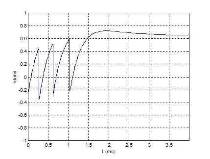
Here is a plot from Part 1, which uses a different phase detector, but has similar pull-in behavior. The plot shows the output of the phase detector during acquisition. As you can see, the PD output is rolling over. Note the dc component is not zero.
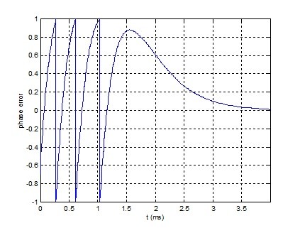
Here is a plot at the output of the integrator. As you can see, Vtune slowly builds towards the required voltage. Once the frequency error is within the loop bandwidth, lock happens quickly.
regards,
Neil
Hi Neil,
thank you so much for your detailed and quick replies to my questions. This series on DPLLs is one of the best, if not the best tutorial I’ve come across in a long time. It is very well written- not to mention your responsiveness in addressing questions that come up- even 4(?) years after the initial posting!. I think the amount and level of detail is just right; well done. I look forward to reading your other articles/tutorials.
Thanks again!
Jorge,
Thanks for the encouragement!
To post reply to a comment, click on the 'reply' button attached to each comment. To post a new comment (not a reply to a comment) check out the 'Write a Comment' tab at the top of the comments.
Please login (on the right) if you already have an account on this platform.
Otherwise, please use this form to register (free) an join one of the largest online community for Electrical/Embedded/DSP/FPGA/ML engineers:


