Working of the first solid state amplifier
Introduction
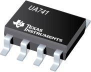
Fig. 1. One of the most popular operational amplifier
Whenever a circuit designer thinks about amplifier, the first think that pops up in his mind is that of operational amplifier (Op-Amp). The answer is simple op-amps are beautiful (literally), you just have to set the gain of the op-amps with pair of resistors and you are good to go. There is always an op-amp for a specific need be it for low-noise application or for rejection of common mode gain. For understanding the electronic amplifier from the first principles, op-amps are no good starting point. Op-amps are built upon abstraction of transistors. Aggregation of transistors makes an op-amp. Let's get on with a transistor.
Transistor
The transistor was invented by three scientists at Bell labs, on December 16, 1947 (year in which India got independence). The scientist on this day had made clever contraption using paper-clip, gold foil and semiconductor material germanium. It could amplify faint electrical signals. It was called point contact transistor. Transistor can be used as both as a amplifier or as a switch. In amplification mode, it amplify electrical signal in switching mode you can switch larger current from lower one.
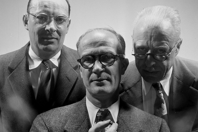
Fig, 2, (L-R) John Bardeen, William Shockley and Walter Brattain
Using transistor as a amplifier is much more elusive then simply using as a switch. Even noble committee was interested in amplification, which you can know after reading the official transcript of the award which says " The Noble prize in physics was awarded jointly to William Bradford Shockley, John Bardeen and Walter Houser Brattain for their research on semiconductors and their discovery of transistor effect. "
Point contact transistor
The first transistor created by trio was point contact transistor. Point contact transistor was predecessor to the commonly used Bipolar Junction Transistor (BJT).
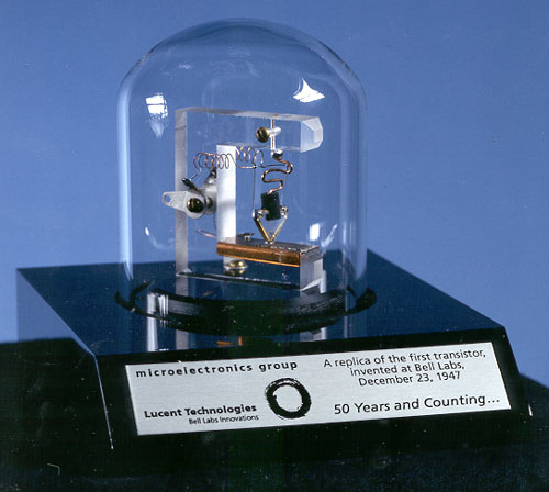
Fig. 3. Replica of the point contact transistor
Working :
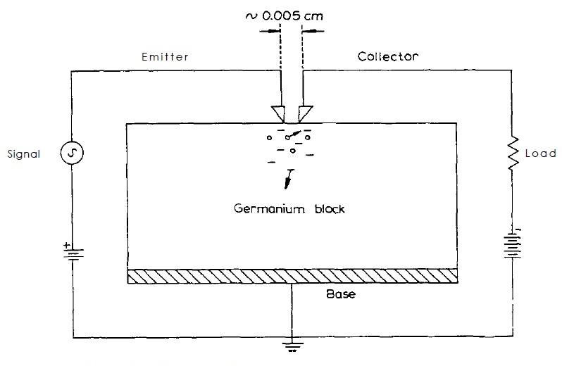
Fig, 4. schematic of the point contact transistor
The emitter and collector are pressed against germanium semiconductor. Thin film of gold foil which is separated by very short gap is used for making emitter and collector terminal, hence the name point contact. The emitter terminal is biased with a d.c voltage, in the forward bias. The base is connected to the germanium block making a low resistance contact with the semiconductor. The collector is connected in the high resistance direction. The crucial bit is : inside semiconductor current is carried by both holes and electrons. If the block of germanium is replaced by any metal, result will be a disaster. A properly doped semiconductor is required for any solid state device operation.
A majority part of forward current consists of holes flowing into the germanium. The current through collector consist of both holes and electrons. But holes cannot flow into the metal contact, hence externally in the circuit current is flowing through electrons only. The collector current is producing electric field in the block, which is attracting holes introduces at the emitter end. Thus a large part of the emitter current flows in the collector circuit, including the signal which needs to be amplified. Thus there is large amplification of the voltage signal.
Useful emitter current can flow through bulk of the semiconductor material, this property is exploited by Shockley to make junction transistor. Point contact transistor is good at showing transistor effect, but making copies of it is impractical. William Shockley invented a new method so that it can be manufactured easily. In junction transistor design minority carries from the emitter diffuse to collector through thin base layer.
Junction transistors have superseded point-contact transistors for most applications. The transistors that you see in real life are all bipolar transistor. Bipolar transistors are used for analog front end design. In the digital domain the bipolar transistors have been replaced by field effect transistor (FET), which is a interesting topic in itself.
References
1) Crystal Fire: The Birth of the Information by Lillian Hoddeson and Michael Riordan
2) Bell Labs Technical journal volume 2, 1948
3) John Bardeen : Nobel lecture Dec 11, 1956
4) A History of the Invention of the Transistor and Where It Will Lead Us, IEEE journal of solid state circuits, volume 32, No 12, Dec 1997
- Comments
- Write a Comment Select to add a comment
To post reply to a comment, click on the 'reply' button attached to each comment. To post a new comment (not a reply to a comment) check out the 'Write a Comment' tab at the top of the comments.
Please login (on the right) if you already have an account on this platform.
Otherwise, please use this form to register (free) an join one of the largest online community for Electrical/Embedded/DSP/FPGA/ML engineers:


